4Kp60 Multi-Sensor HDR Camera Solution System Example Design for Agilex™ 5 Devices
The design is compatible with Altera® Quartus® Prime Pro Edition version 25.1 Linux.
Overview
The 4K Multi-Sensor HDR Camera Solution System Example Design for Agilex™ 5 Devices demonstrates a practical glass-to-glass camera solution. The exclusive support for industry-standard Mobile Industry Processor Interface (MIPI) D-PHY and MIPI CSI-2 interface on Agilex™ 5 FPGAs provides a powerful tool for camera product development. The MIPI interface supports up to 2.5Gbps per lane and up to 8x lanes per MIPI interface enables seamless data reception from multiple 4K image sensors to the FPGA fabric for further processing. Each MIPI CSI-2 IP instance converts pixel data to AXI4-Streaming outputs, enabling connectivity to other IP cores within Altera®'s Video and Vision Processing (VVP) Suite.
The design is a hardware-software co-design, whose hardware component comprises an Image Signal Processor (ISP), various VVP IPs, Hard Processor Subsystem (HPS) and various connectivity IPs. The software stack is Linux based and runs on the HPS.
The hardware includes a multi-sensor input video switch feeding into an Image Signal Processing (ISP) subsystem. The ISP is a video processing pipeline incorporating many VVP IP cores such that the raw sensor image data can be processed into RGB video data. The backend of the ISP pipeline also includes adaptive local tone mapping (TMO) for handling wide dynamic range scenes, 1D-LUT and 3D-LUT IPs for color transformations and High Dynamic Range (HDR) conversion, and a high-performance Warp IP core for geometric distortion correction. The design drives the resulting 4Kp60 streaming video output data through an Altera® DisplayPort IP.
The software stack consists of an application software binary running on Linux operating system with various layers of drivers. The backend part of the application software interrogates the hardware, discovers the IP components dynamically and configures them. Multiple feedback loops monitor the hardware and keep various hardware components in lockstep. Some of the notable feedback loops are Automatic White Balance (AWB), Auto Exposure (AE), and Adaptive Noise Reduction (ANR) algorithms, reading their relevant statistics and adjusting various coefficients and Look Up Tables (LUTs) in real time. The frontend of the software creates a web based Graphical User Interface (GUI) and runs it over a web server.
The following diagrams provide an overview of the interaction of software running on ARM CPUs inside the Hard Processor Subsystem (HPS) and hardware components running in the programmable logic parts of the device. (For more information of ARM HPS in Altera® Agilex™ Devices refer to the User Manuals section.)
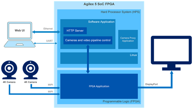
High-Level Block Diagram of the 4Kp60 Multi-Sensor HDR Camera Solution System Example Design
Pre-requisites
Hardware Requirements
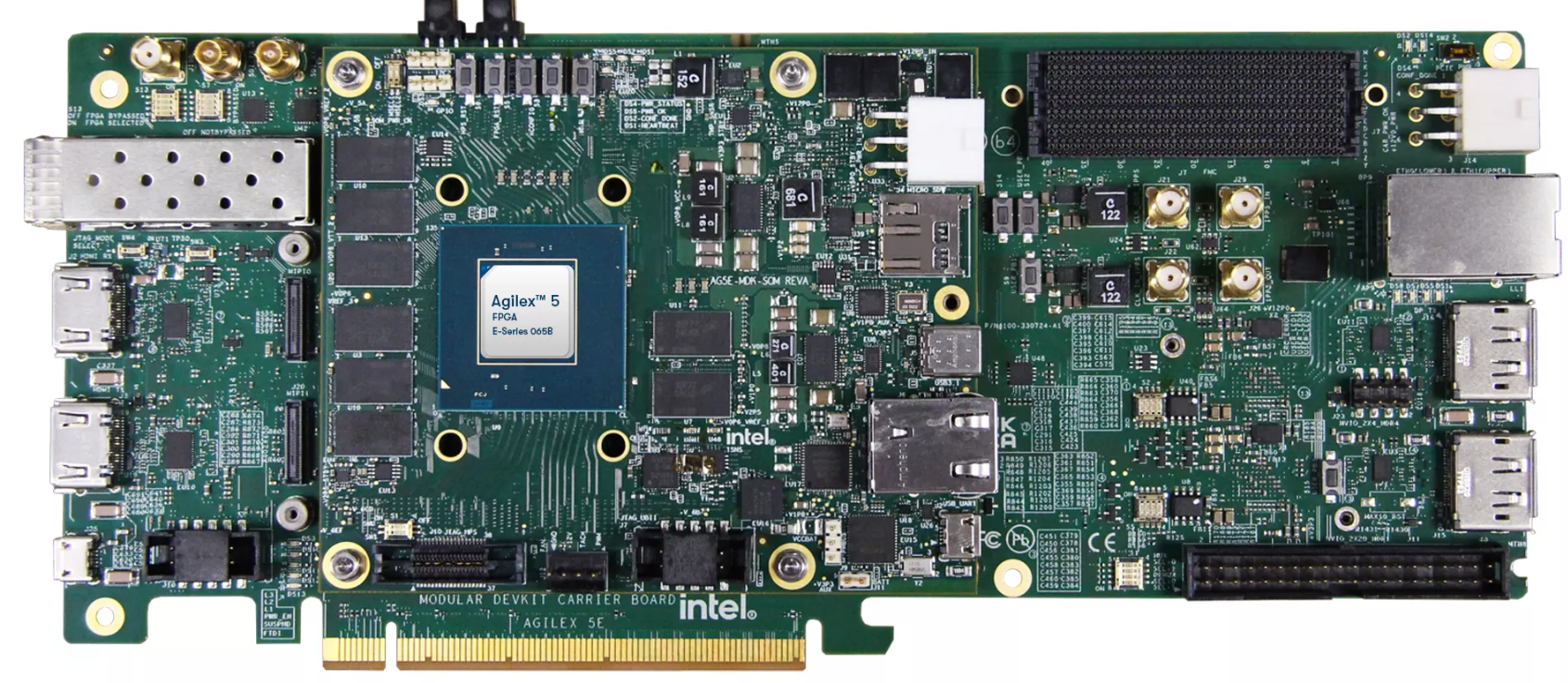
Agilex™ 5 FPGA E-Series 065B Modular Development Kit
- 1 or 2 Framos FSM:GO IMX678C Camera Modules, with:
- Mount/Tripod
- A Framos cable for PixelMate MIPI-CSI-2 for each Camera Module:
- Minimum 8GB U3 microSD Card.
- DP Cable or HDMI Cable (with 4Kp60 Converter Dongle).
- USB Micro B JTAG Cable (for JTAG programming).
- USB Micro B Serial Cable (for HPS terminal connection).
- RJ45 Ethernet Cable (HPS network connection).
- Monitor/TV (recommend 4Kp60 capable).
Software Requirements to run
- Host PC with:
- 8 GB of RAM (less if not rebuilding binaries).
- Linux/Windows OS installed.
- Serial terminal (such as GtkTerm or Minicom on Linux, and TeraTerm or
PuTTY on Windows).
- FTDI FT232R USB UART drivers (for a Windows host).
- Tool to write images for removable USB drives or microSD cards such as Win32DiskImager on Windows or "dd" command on Linux.
- Altera® Quartus® Prime Pro Edition version 25.1 Programmer and Tools.
- Ethernet connection (either direct from Host PC to development board, or
via a switch or router).
- Note, you may need to disconnected/disabled VPN if it is installed on the Host PC.
- Web browser.
Download the pre-built Binaries
- Download the Agilex™ 5 Modular Development board binaries:
Binaries
| Source | Link | Description |
|---|---|---|
| QSPI | top.core.jic | Allows the development board to be booted from the microSD card |
| microSD Card Image | hps-first-vvp-isp-demo-image-agilex5_mk_a5e065bb32aes1.wic.gz | The complete Camera Solution System Example Design |
Getting Started - run with pre-built binaries
Follow the instructions provided in this section to run the 4K Multi-Sensor HDR Camera Solution System Example Design on the Agilex™ 5 FPGA E-Series 065B Modular Development Kit.
Programming
Setting Up your Modular Development Board
Warning
Handle ESD-sensitive equipment (boards, microSD Cards, Camera sensors, etc.) only when properly grounded and at an ESD-safe workstation
- Configure the board switches as shown:
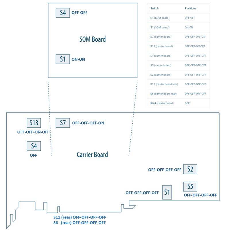
Modular Development Board - Default Switch Positions
Main switch configurations used by the Camera Solution System Example Design
JTAG Mode: SOM S4=OFF:OFF, or
ASx4 (QSPI) Mode: SOM S4=ON:ON
- Connect micro USB cable between the carrier board (
J35) and the Host PC. This will be used for JTAG communication. Look at what ports are enumerated on your Host computer. There should be a series of four. - Connect micro USB cable between the SOM board (
J2, HSP_UART) and the Host PC. This will be used for HPS UART communication. Look at what ports are enumerated on your Host computer. There should be a series of four. Use the 3rd one in the list as the HPS serial port. - Connect an RJ45 cable between the ethernet port on the SOM board (
J6, ETH 1G HPS) and make sure it is on the same network as your Host PC. You can check theeth0IP address after boot using the Linuxip acommand.
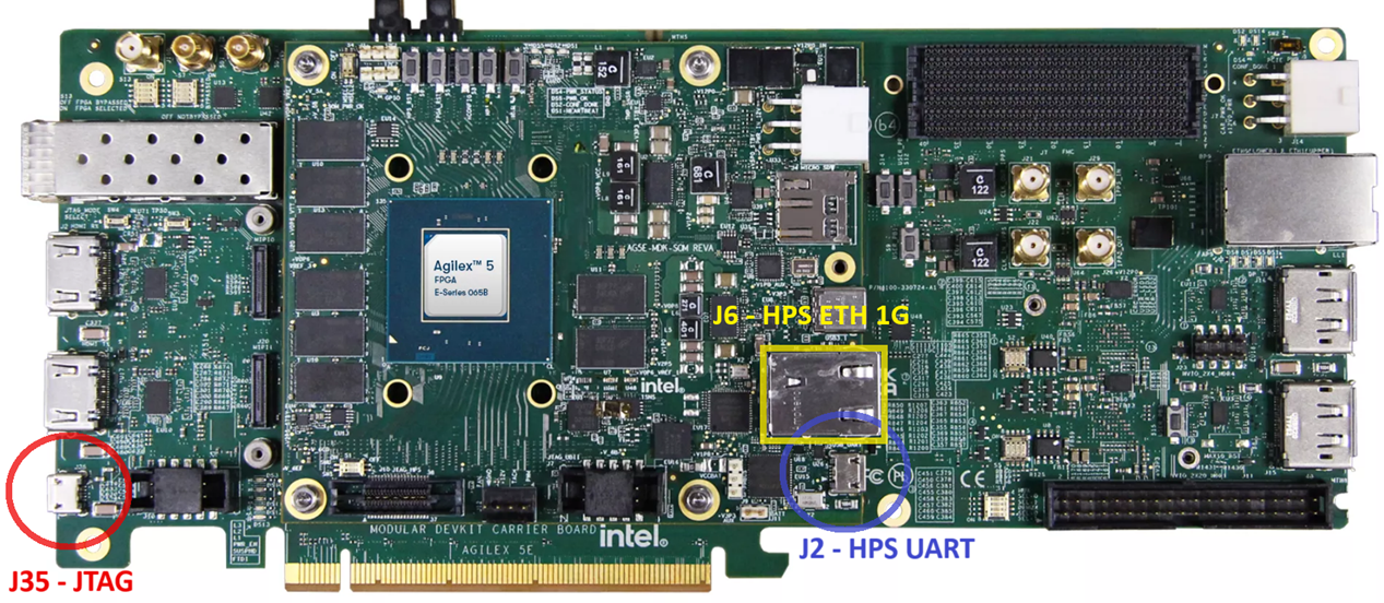
Board Connections
Burn the microSD Card Image
- Either use your own or download the pre-built
<name>.wic.gzimage. -
Extract
<name>.wicimage from the zip file- On Linux, use the
ddutility:
- On Windows, use the 7-Zip program (or similar):
- Right click
<name>.wic.gzfile, and select "Extract All..."
- Right click
- On Linux, use the
-
Write the
<name>.wicimage to the microSD card using a USB writer:- On Linux, use the
ddutility:
# Determine the device associated with the SD card on the host computer. cat /proc/partitions # This will return for example /dev/sd<x> # Use dd to write the image in the corresponding device sudo dd if=<name>.wic of=/dev/sd<x> bs=1M # Flush the changes to the microSD card sync-
On Windows, use the Win32DiskImager program (or similar):
- Click browse icon and select "*.*" filter:
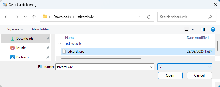
Navigate to your download and select
<name>.wicin the "Disk Imager" tool
- Write the image (note your Device may be different to that shown):
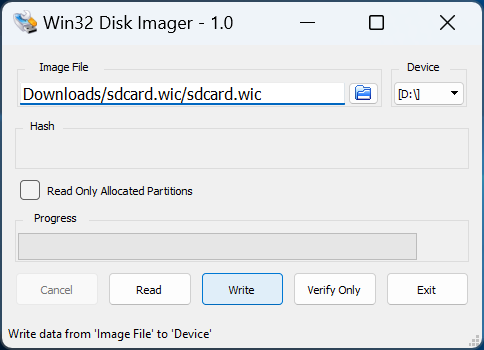
Write the microSD Card using the "Disk Imager" tool
- On Linux, use the
- Turn off the board and insert the microSD card in the microSD card slot located on the SOM board.
Program the QSPI Flash Memory
This should only need to be done once. To program the QSPI flash memory:
- Power down the board. Set MSEL=JTAG by setting the S4 dip switch
on the SOM to OFF-OFF.
- This prevents any bootloader from starting and leaves the JTAG chain in a default state.
- Power up the board.
- Either use your own or download the pre-built
JICimage, and write it to the QSPI Flash memory using either the command:
-
or, optionally using the Quartus® Programmer GUI:
- Launch the Quartus® Programmer and Configure the "Hardware Setup..."
settings as following:
- Launch the Quartus® Programmer and Configure the "Hardware Setup..."
settings as following:
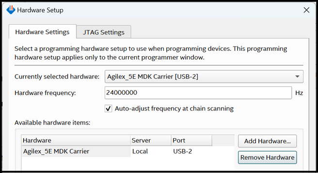
Programmer - GUI Hardware Settings
- Click "Auto Detect", select the device
A5EC065BB32AR0, and press "Change File.."
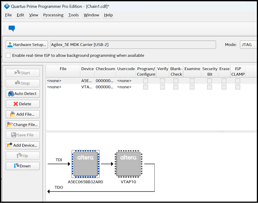
Programmer - After "Auto Detect"
Select your top.core.jic file. The MT25QU02G device should be shown (see
below). Check the "Program/Configure" box and press the "Start" button.
Wait until the programming has been completed (which can take several minutes).
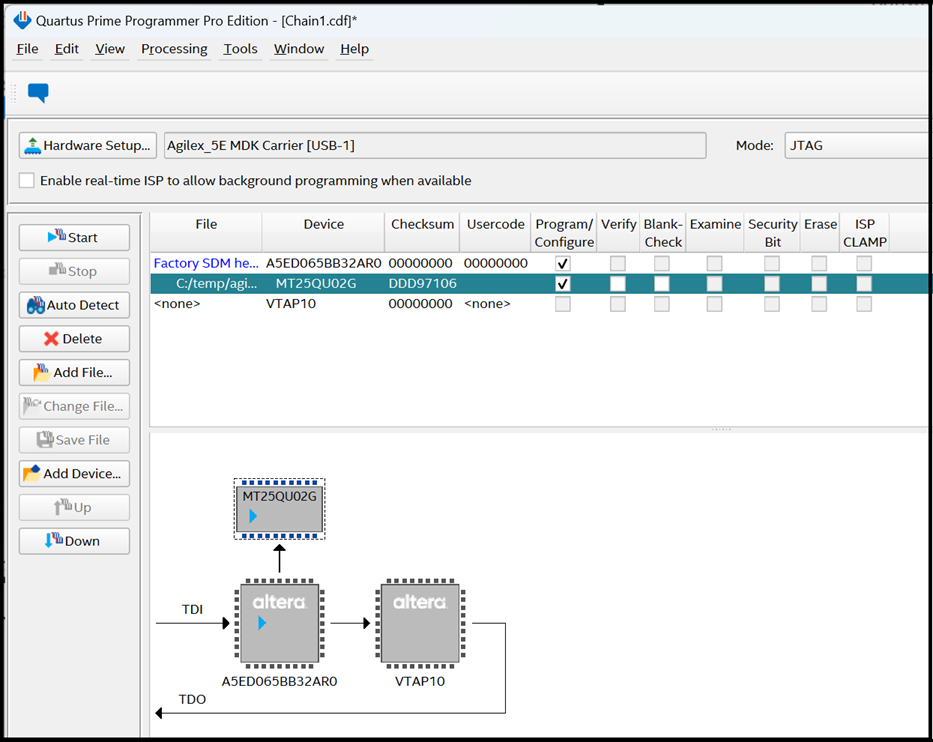
Programming the QSPI Flash with the JIC file
- Power down the board. Set MSEL=ASX4 (QSPI) by setting the S4 dip switch
on the SOM to ON-ON.
- This starts the HPS bootloader and FPGA configuration from the microSD Card
after power up.
- This starts the HPS bootloader and FPGA configuration from the microSD Card
after power up.
Running
Board and Host PC Setup
Warning
Handle ESD-sensitive equipment (boards, microSD Cards, Camera sensors, etc.) only when properly grounded and at an ESD-safe workstation
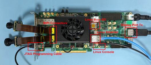
Make the required connections between the Host PC and the Modular Development board as shown in the following diagram:
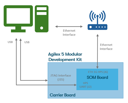
Development Kit and Host PC Connection diagram
- Connect the Framos cable(s) between the Framos Camera Module(s) and the Modular Development board taking care to align the cable(s) correctly with the connectors (pin 1 to pin 1). For a single camera module, either MIPI connector can be used.
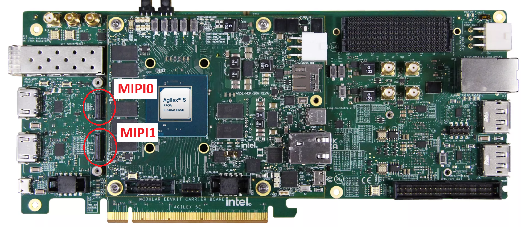
Board MIPI connections
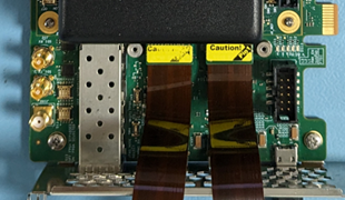
Board MIPI and Ribbon Cable
Camera and Ribbon Cable
Board with Connections
- Connect the Modular Development carrier board DisplayPort Tx connector to the Monitor using a suitable cable (and dongle if you are using HDMI).
Connect Browser to UI
- Power up the board (if not already powered) and set up the serial terminal emulator (minicom,
teraterm, putty, etc.):
- Select the correct
COMxport. (The Modular Development board presents 4 serial COM ports over a single connection and the Linux system uses the 3rd port in order). Set the port configuration as follows:- 115200 baud rate, 8 Data bits, 1 Stop bit, CRC and Hardware flow control disabled.
- Select the correct
- The Linux OS will boot and the 4K Multi-Sensor HDR Camera Solution System Example Design Application should run automatically.
- A few seconds after Linux boots, the application will detect the attached Monitor and the ISP processed output will be displayed using the best supported format.
-
Take note of the board's IP address.
-
The board's IP address can also be found using the terminal by logging in as
root(no password required) and querying the Ethernet controller:
eth0provides the IPv4 or IPv6 address to connect to.
-
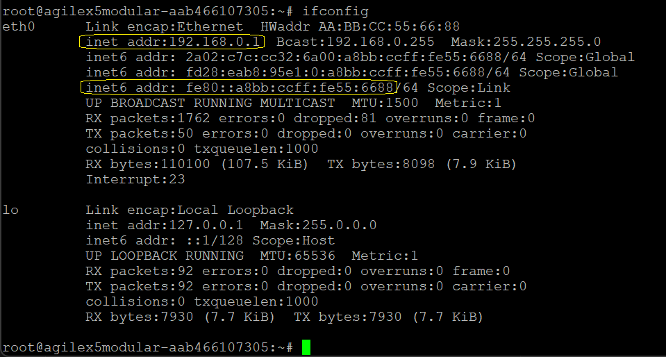
Example ifconfig output for if network provides DHCP
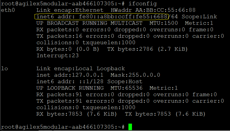
Example ifconfig output for if no DHCP support, or direct connection
- Connect your web browser to the boards IP address so you can interact with
the 4K Multi-Sensor HDR Camera Solution System Example Design using the GUI.
- To connect using IPv6 for the examples above you would use
http://[fe80::a8bb:ccff:fe55:6688](note the square brackets) - To connect using IPv4 for the DHCP example above you would use
http://192.168.0.1
- To connect using IPv6 for the examples above you would use

Example web browser URL for IPv6 address

Example web browser URL for IPv4 address
- During connection, you will see the Altera® splash screen, after which you will be presented with the Web GUI:
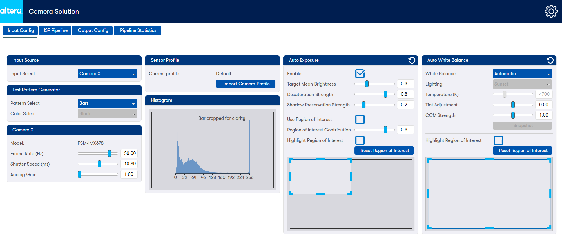
Example Camera Solution GUI
Recommended User Flows
Sources
The sources listed in this table are the most current and highly recommended for Quartus® 25.1 builds. Users are advised to utilize the updated versions of these building blocks in production environments. Please note that this is a demonstration design and is not suitable for production or final deployment.
System Example Design Source Repository
| Component | Location | Branch |
|---|---|---|
| Assets Release Tag | https://github.com/altera-fpga/agilex-ed-camera/releases/tag/rel-25.1 | rel-25.1 |
| Repository | https://github.com/altera-fpga/agilex-ed-camera | rel-25.1 |
With the available resources, you can create and modify, build and compile, and execute the 4K Multi-Sensor HDR Camera Solution System Example Design. There are 3 recommended flows that you can explore:
- User Flow 1: Getting Started - Running with pre-built binaries.
- User Flow 2: Use the SOF Modular Design Toolkit (MDT) Flow - typically used for Quartus® with OpenCore Plus IP Evaluation License for time limited and tethered camera solutions.
- User Flow 3: Use the RBF Modular Design Toolkit (MDT) Flow - typically used for Quartus® with full IP License for turnkey microSD card camera solutions.
Note
The free OpenCore Plus feature allows you to evaluate licensed IP cores in
simulation and hardware before purchase. OpenCore Plus evaluation supports
the following two operation modes:
Untethered — run the design containing the licensed IP for a limited time.
Tethered — run the design containing the licensed IP for a longer time or
indefinitely. This operation requires a JTAG connection between your board
and the Host computer.
Note: All IP cores that use OpenCore Plus time out simultaneously when any
IP core in the design times out.
Flows
Recommended User Flows
Camera Solution System Example Design - Documentation
- Features.
- ISP Functional Description.
- FPGA Hardware Functional Description.
- Software Functional Description.
- Web GUI Functional Description.
- Design Security Considerations.
- Acronyms and Terminology.
Camera Solution System Example Design - References
- Agilex™ 5 FPGA E-Series 065B Modular Development Kit Product Brief.
- Framos FSM:GO IMX678C Camera Modules.
- Video and Vision Processing Suite Altera® FPGA IP User Guide.
- VVP IP Suite, VVP Tone Mapping Operator (TMO) IP, VVP Warp IP, and 3D LUT IP.
- MIPI DPHY IP and MIPI CSI-2 IP.
- Nios® V Processor.
Other Repositories Used
| Component | Location | Branch |
|---|---|---|
| Modular Design Toolkit | https://github.com/altera-fpga/modular-design-toolkit | rel-25.1 |
| Linux | https://github.com/altera-opensource/linux-socfpga | socfpga-6.6.22-lts |
| Arm Trusted Firmware | https://github.com/ARM-software/arm-trusted-firmware | socfpga_v2.11.0 |
| U-Boot | https://github.com/altera-opensource/u-boot-socfpga | v2024.01 |
| Yocto Project: poky | https://git.yoctoproject.org/poky | scarthgap |
Useful User Manuals and Reference Materials
- Hard Processor System Technical Reference Manual: Agilex™ 5 SoCs (25.1).
- NiosV Processor for Altera® FPGA.
- Agilex™ 5 FPGA E-Series 065B Modular Development Kit.
Notices & Disclaimers
Altera® Corporation technologies may require enabled hardware, software or service activation. No product or component can be absolutely secure. Performance varies by use, configuration and other factors. Your costs and results may vary. You may not use or facilitate the use of this document in connection with any infringement or other legal analysis concerning Altera or Intel products described herein. You agree to grant Altera Corporation a non-exclusive, royalty-free license to any patent claim thereafter drafted which includes subject matter disclosed herein. No license (express or implied, by estoppel or otherwise) to any intellectual property rights is granted by this document, with the sole exception that you may publish an unmodified copy. You may create software implementations based on this document and in compliance with the foregoing that are intended to execute on the Altera or Intel product(s) referenced in this document. No rights are granted to create modifications or derivatives of this document. The products described may contain design defects or errors known as errata which may cause the product to deviate from published specifications. Current characterized errata are available on request. Altera disclaims all express and implied warranties, including without limitation, the implied warranties of merchantability, fitness for a particular purpose, and non-infringement, as well as any warranty arising from course of performance, course of dealing, or usage in trade. You are responsible for safety of the overall system, including compliance with applicable safety-related requirements or standards. © Altera Corporation. Altera, the Altera logo, and other Altera marks are trademarks of Altera Corporation. Other names and brands may be claimed as the property of others.
OpenCL* and the OpenCL* logo are trademarks of Apple Inc. used by permission of the Khronos Group™.
Created: October 6, 2025