HPS GSRD User Guide
Overview
The HPS Baseline System Example Design (formerly known as "GSRD" or "Golden System Reference Design") demonstrates basic HPS functionality on the Altera® Agilex™ 7 FPGA F-Series Transceiver-SoC Development Kit (P-Tile and E-Tile)
The design is comprised of the following components:
- Quartus Design
- HPS Software
- Arm Trusted Firmware
- U-Boot
- Linux Kernel
- Linux Drivers
- Sample Applications
Prerequisites
The following are required in order to be able to fully exercise the System Example Design:
- Agilex™ 7 FPGA F-Series Transceiver-SoC Development Kit (P-Tile and E-Tile) ordering code DK-SI-AGF014EB
- SD/MMC HPS Daughtercard
- SDM QSPI Bootcard
- Mini USB cable for serial output
- Micro USB cable for on-board Altera® FPGA Download Cable II
- Micro SD card (4GB or greater)
- Host PC with
- Linux - Ubuntu 22.04LTS was used to create this page, other versions and distributions may work too
- Serial terminal (for example Minicom on Linux and TeraTerm or PuTTY on Windows)
- Micro SD card slot or Micro SD card writer/reader
- Altera® Quartus® Prime Pro Edition Version 26.3
- Local Ethernet network, with DHCP server (will be used to provide IP address to the board)
You can determine your board version by referring to the following table from https://docs.altera.com/r/docs/683752/current/agilextm-7-fpga-f-series-transceiver-soc-development-kit-user-guide/overview
| Development Kit Version | Ordering Code | Device Part Number | Starting Serial Number |
|---|---|---|---|
| Altera® Agilex™ 7 FPGA F-Series Transceiver-SoC Development Kit (Production 2 P-Tiles & E-Tiles) | DK-SI-AGF014EB | AGFB014R24B2E2V (Power Solution 2) | 00205001 |
| Altera® Agilex™ 7 FPGA F-Series Transceiver-SoC Development Kit (Production 1 P-Tiles & E-Tiles) | DK-SI-AGF014EA | AGFB014R24B2E2V (Power Solution 1) | 0001101 |
| Altera® Agilex™ 7 FPGA F-Series Transceiver-SoC Development Kit (ES P-Tiles & E-Tiles) | DK-SI-AGF014E3ES | AGFB014E3ES (Power Solution 1) | 0001001 |
The DK-SI-AGF014E3ES and DK-SI-AGF014EA are deprecated, and not supported anymore.
The U-Boot and Linux compilation, Yocto compilation and creating the SD card image require a Linux host PC. The rest of the operations can be performed on either a Windows or Linux host PC.
Release Contents
Release Notes
The Altera® FPGA HPS Embedded Software release notes can be accessed from the following link: https://github.com/altera-fpga/gsrd-socfpga/releases/tag/QPDS26.3_REL_BASELINE_PR
Prebuilt Binaries
SD Card Boot
The release files are accessible at https://releases.rocketboards.org/2026.10/gsrd/agilex7_dk_si_agf014eb_gsrd/
The source code is also included on the SD card in the Linux rootfs path /home/root:
| File | Description |
|---|---|
| linux-socfpga-v6.18.37-lts-src.tar.gz | Source code for Linux kernel |
| u-boot-socfpga-v2026.07-src.tar.gz | Source code for U-Boot |
| arm-trusted-firmware-v2.15.0-src.tar.gz | Source code for Arm Trusted Firmware |
QSPI Boot
The release files are accessible at https://releases.rocketboards.org/2026.10/qspi/agilex7_dk_si_agf014eb_qspi/.
NAND Boot
The release files are accessible at https://releases.rocketboards.org/2026.10/nand/agilex7_dk_si_agf014eb_nand/
eMMC Boot
The release files are accessible at https://releases.rocketboards.org/2026.10/emmc/agilex7_dk_si_agf014eb_emmc/
Component Versions
Altera® Quartus® Prime Pro Edition Version 26.3 and the following software component versions integrate the 26.3 release.
| Component | Location | Branch | Commit ID/Tag |
|---|---|---|---|
| HPS Baseline System Example Design | https://github.com/altera-fpga/agilex7-ed-hps-baseline | main | QPDS26.3_REL_BASELINE_PR |
| Linux | https://github.com/altera-fpga/linux-socfpga | socfpga-6.18.37-lts | QPDS26.3_REL_BASELINE_PR |
| Arm Trusted Firmware | https://github.com/altera-fpga/arm-trusted-firmware | socfpga_v2.15.0 | QPDS26.3_REL_BASELINE_PR |
| U-Boot | https://github.com/altera-fpga/u-boot-socfpga | socfpga_v2026.07 | QPDS26.3_REL_BASELINE_PR |
| Yocto Project | https://git.yoctoproject.org/poky | wrynose | latest |
| Yocto meta-altera-fpga Layer | https://github.com/altera-fpga/meta-altera-fpga | wrynose | QPDS26.3_REL_BASELINE_PR |
| KAS | https://github.com/siemens/kas/ | master | 5.4 |
Note: The combination of the component versions indicated in the table above has been validated through the use cases described in this page and it is strongly recommended to use these versions together. If you decided to use any component with different version than the indicated, there is not warranty that this will work.
Note: Starting from 26.3 Quartus release, the build of the Quartus projects in the System Example Designs are based only on Visual Designer Studio (VDS).
Please review the following KDB if you face Quartus design build problems when the RTL was generated with VDS:
Why do Quartus® Prime Pro 26.3 and earlier fail to build a Agilex® 5/Agilex® 3/Agilex® 7 FPGA M-Series VDS based design whose RTL has been generated with VDS?.
Quartus Design Overview
The Quartus Design is an important part of the System Example Design and consists of the following components:
- Hard Processor System (HPS)
- Quad Arm Cortex-A53 MPCore Processor
- HPS Peripherals connected to Out-of-Box Experience (OOBE) Daughter Card:
- Micro SD for HPS storage
- EMAC
- HPS JTAG debug
- I2C
- USB UART
- USB 2.0 OTG
- Two Push buttons and Three LEDs
- Hard Memory Controller (HMC) for HPS External Memory Interface (EMIF)
- FPGA Peripherals connected to Lightweight HPS-to-FPGA (LWH2F) AXI Bridge and JTAG to Avalon Master Bridge
- Three user LED outputs
- Four user DIP switch inputs
- Four user push-button inputs
- Interrupt Latency Counter
- System ID
- FPGA Peripherals connected to HPS-to-FPGA (H2F) AXI Bridge
- 256KB of FPGA on-chip memory
- JTAG to Avalon Master Bridges connected to:
- FPGA-to-SDRAM 0/½ Interfaces
- FPGA-to-HPS AXI Bridge
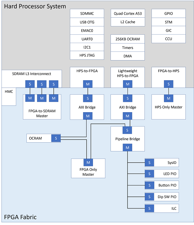
The Quartus Design allows hardware designers to access each peripheral in the FPGA portion of the SoC with System Console, through the JTAG master module. This signal-level access is independent of the driver readiness of each peripheral.
MPU Address Maps
This section presents the address maps as seen from the MPU (Cortex-A53) side.
HPS-to-FPGA Address Map
The MPU region provide windows of 4 GB into the FPGA slave address space. The lower 1.5 GB of this space is mapped to two separate addresses - firstly from 0x8000_0000 to 0xDFFF_FFFF and secondly from 0x20_0000_0000 to 0x20_5FFF_FFFF. The following table lists the offset of each peripheral from the HPS-to-FPGA bridge in the FPGA portion of the SoC.
| Peripheral | Address Offset | Size (bytes) | Attribute |
|---|---|---|---|
| onchip_memory2_0 | 0x0 | 256K | On-chip RAM as scratch pad |
Lightweight HPS-to-FPGA Address Map
The the memory map of system peripherals in the FPGA portion of the SoC as viewed by the MPU (Cortex-A53), which starts at the lightweight HPS-to-FPGA base address of 0xF900_0000, is listed in the following table.
| Peripheral | Address Offset | Size (bytes) | Attribute |
|---|---|---|---|
| sysid | 0x0000_0000 | 8 | Unique system ID |
| led_pio | 0x0000_1080 | 16 | LED outputs |
| button_pio | 0x0000_1060 | 16 | Push button inputs |
| dipsw_pio | 0x0000_1070 | 16 | DIP switch inputs |
| ILC | 0x0000_1100 | 256 | Interrupt latency counter (ILC) |
JTAG Master Address Map
There are two JTAG master interfaces in the design, one for accessing non-secure peripherals in the FPGA fabric, and another for accessing secure peripheral in the HPS through the FPGA-to-HPS Interface.
The following table lists the address of each peripheral in the FPGA portion of the SoC, as seen through the non-secure JTAG master interface.
| Peripheral | Address Offset | Size (bytes) | Attribute |
|---|---|---|---|
| onchip_memory2_0 | 0x0000_0000 | 256K | On-chip RAM |
| sysid | 0x0004_0000 | 8 | Unique system ID |
| led_pio | 0x0004_0080 | 16 | LED outputs |
| button_pio | 0x0004_0060 | 16 | Push button inputs |
| dipsw_pio | 0x0004_0070 | 16 | DIP switch inputs |
| ILC | 0x0004_0100 | 256 | Interrupt latency counter (ILC) |
Interrupt Routing
The HPS exposes 64 interrupt inputs for the FPGA logic. The following table lists the interrupt connections from soft IP peripherals to the HPS interrupt input interface.
| Peripheral | Interrupt Number | Attribute |
|---|---|---|
| dipsw_pio | f2h_irq0[0] | 4 DIP switch inputs |
| button_pio | f2h_irq0[1] | 4 Push button inputs |
The interrupt sources are also connected to an interrupt latency counter (ILC) module in the system, which enables System Console to be aware of the interrupt status of each peripheral in the FPGA portion of the SoC.
Typical HPS Boot Flow
The boot flow includes the following stages:
1. SDM
2. U-Boot SPL
3. ATF
4. U-Boot
5. Linux
6. Application

The following table presents a short description of the different boot stages:
| Stage | Description |
|---|---|
| SDM | Secure Device Manager boots first |
| U-Boot SPL | Configures IO, FPGA, brings up SDRAM |
| ATF | Arm Trusted Firmware, provides SMC handler |
| U-Boot | Loads Linux kernel |
| Linux | Operating system |
| Application | User application |
For more information, please refer to Altera® Agilex™ 7 Hard Processor System Technical Reference Manual (Booting and Configuration chapter).
Exercise Prebuilt Binaries
Configure Board
This section presents the necessary board settings in order to run the System Example Design on the development board.
First, confirm the following:
- SD Card/OOBE Daughter card is installed on HPS Daughter card socket
Then the board switches need to be configured as follows:
- SW1: ON-OFF-OFF-ON
- SW2: all OFF
- SW3: OFF-OFF-ON-ON-ON-ON
- SW4: OFF-OFF-OFF-ON
- SW5: all OFF
- SW6: OFF-OFF-OFF-ON
- SW9: OFF-OFF
- SW10: OFF-ON
Configure Serial Connection
The HPS Enablement Daughtercard has a built-in FTDI USB to Serial converter chip that allows the host computer to see the board as a virtual serial port. Ubuntu and other modern Linux distributions have built-in drivers for the FTDI USB to Serial converter chip, so no driver installation is necessary on those platforms. Microsoft Windows 10 and 11 automatically install the necessary drivers.
The serial communication parameters are:
- Baud-rate: 115,200
- Parity: none
- Flow control: none
- Stop bits: 1
On Windows, utilities such as TeraTerm and PuTTY can be used to connect to the board. They are easily configured from the tool menus.
On Linux, the minicom utility can be used. Here is how to configure it:
The virtual serial port is usually named /dev/ttyUSB0. In order to determine the device name associated with the virtual serial port on your host PC, please perform the following:
- Use the following command to determine which USB serial devices are already installed:
ls /dev/ttyUSB* - Connect mini USB cable from J7 to the PC. This will enable the PC to communicate with the board, even if the board is not powered yet.
- Use the
ls /dev/ttyUSB*command command again to determine which new USB serial device appeared. - Install minicom application on host PC, if not installed:
- On Ubuntu, use
sudo apt-get install minicom
- On Ubuntu, use
- Configure minicom with the next command:
Under Serial Port Setup choose the following:
- Serial Device: /dev/ttyUSB0 (edit to match the system as necessary)
- Bps/Par/Bits: 115200 8N1
- Hardware Flow Control: No
- Software Flow Control: No
- Hit [ESC] to return to the main configuration menu
Select Save Setup as dfl to save the default setup. Then select Exit.
Boot from SD Card
This section presents how to write the QSPI Falsh and SD Card image files, configure the board and boot Linux.
Write QSPI Image
The QSPI JIC image contains the FPGA configuration bitstream, and the U-Boot SPL.
1. Download and extract the image file:
cd $TOP_FOLDER
wget https://releases.rocketboards.org/2026.10/gsrd/agilex7_dk_si_agf014eb_gsrd/ghrd.hps.jic
2. Configure MSEL to JTAG:
- SW1: ON-ON-ON-ON
3. Power cycle the board
4. Write the image using the following commands:
5. Configure MSEL back to QSPI:
- SW1: ON-OFF-OFF-ON
Write SD Card Image
This section explains how to create the SD card necessary to boot Linux, using the SD card image available with the pre-built Linux binaries package. Once the SD card has been created, insert the card into the SD slot of the Micro SD daughter card.
Write SD Card on Linux
1. Download the SD card image and extract it:
wget https://releases.rocketboards.org/2026.10/gsrd/agilex7_dk_si_agf014eb_gsrd/sdimage.tar.gz
tar xf sdimage.tar.gz
The extracted file is named gsrd-console-image-agilex7.rootfs.wic.
2. Determine the device associated with the SD card on the host by running the following command before and after inserting the card.
Let's assume it is /dev/sdx.
3. Use dd utility to write the SD image to the SD card.
Note we are using sudo to be able to write to the card.
4. Use sync utility to flush the changes to the SD card.
Write SD Card on Windows
1. Download the SD card image and extract it: https://releases.rocketboards.org/2026.10/gsrd/agilex7_dk_si_agf014eb_gsrd/sdimage.tar.gz
The extracted file is named gsrd-console-image-agilex7.rootfs.wic.
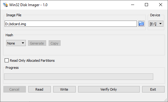
2. Rename the wic file as sdcard.img
3. Use Win32DiskImager to write the image to the SD card. The tool can be downloaded from https://sourceforge.net/projects/win32diskimager/files/latest/download
Boot Linux
This section presents how to boot Linux on the board. The required steps are:
1. Start serial terminal (when using Minicom it will connect using the selected settings, for others connect manually).
2. Power up the board.
3. U-Boot SPL is ran
4. U-Boot is ran
5. Linux boots.
6. Login using 'root' and no password.
7. Run 'ifconfig' command to determine the IP of the board
root@agilex7dksiagf014eb:~# ifconfig
eth0: flags=4163 mtu 1500
 inet 192.168.1.163 netmask 255.255.255.0 broadcast 192.168.1.255
 inet6 fe80::20cd:5eff:fe36:dbaf prefixlen 64 scopeid 0x20
 ether 22:cd:5e:36:db:af txqueuelen 1000 (Ethernet)
 RX packets 14 bytes 2126 (2.0 KiB)
 RX errors 0 dropped 0 overruns 0 frame 0
 TX packets 43 bytes 7513 (7.3 KiB)
 TX errors 0 dropped 0 overruns 0 carrier 0 collisions 0
 device interrupt 21 base 0x2000

eth1: flags=4099 mtu 1500
 ether 5a:4d:ca:de:cd:f6 txqueuelen 1000 (Ethernet)
 RX packets 0 bytes 0 (0.0 B)
 RX errors 0 dropped 0 overruns 0 frame 0
 TX packets 0 bytes 0 (0.0 B)
 TX errors 0 dropped 0 overruns 0 carrier 0 collisions 0
 device interrupt 22 base 0xc000

lo: flags=73 mtu 65536
 inet 127.0.0.1 netmask 255.0.0.0
 inet6 ::1 prefixlen 128 scopeid 0x10
 loop txqueuelen 1000 (Local Loopback)
 RX packets 100 bytes 8468 (8.2 KiB)
 RX errors 0 dropped 0 overruns 0 frame 0
 TX packets 100 bytes 8468 (8.2 KiB)
 TX errors 0 dropped 0 overruns 0 carrier 0 collisions 0
Note: there are two IP addresses, one coming from the Ethernet port on the HPS Daughtercard, and one from the Ethernet port on the DevKit, which is connected throgh SGMII.
Run Sample Applications
The System Example Design includes a number of sample Linux applications that help demonstrate some of the features of the platform:
- Display Hello World message
- Control LEDs
- Detect interrupts from push buttons and DIP switches
The sample applications can be used as a starting point for users to write their own applications that interact with software IP through Linux drivers.
Prerequisites
1. Boot Linux on the target board as described in Boot Linux. You will not need to use the serial terminal if you plan on using ssh connection.
2. Connect to the board using one of the following options:
- Connect using serial console, as described in Boot Linux
- Connect using ssh, as described in Connect With SSH
3. In serial console, or ssh client console, change current folder to be /home/root/alteraFPGA. This is where the application binaries are stored.
Display Hello World Message
Run the following command to display the Hello World message on the console:
Exercise Soft PIO Driver for LED Control
The following LEDs are exercised:
| User FPGA LED Number | Corresponding Board LED |
|---|---|
| 0 | D21 |
| 1 | D23 |
| 2 | D25 |
Note: User FPGA LED #3 / D27 is quickly blinking, and cannot be controlled from software.
1. In order to blink an LED in a loop, with a specific delay in ms, run the following command:
- The led_number specifies the desired LED, and is a value between 0 and 3.
- The delay_ms is a number that specifies the desired delay in ms between turning the LED on and off.
2. In order to turn an individual LED on or off, run the following command:
- The led_number specifies the desired LED, and is a value between 0 and 3.
- The state needs to be 0 to turn the LED off, and 1 to turn the LED on.
3. In order to scroll the FPGA LEDs with a specific delay, please run the following command:
The delay specifies the desired scrolling behavior:
- delay > 0 - specify new scrolling delay in ms, and start scrolling
- delay < 0 - stop scrolling
- delay = 0 - display current scroll delay
System Check Application
System check application provides a glance of system status of basic peripherals such as:
- USB: USB device driver
- Network IP (IPv4): Network IP address
- HPS LEDs: HPS LED state
- FPGA LEDs: FPGA LED state
Run the application by issuing the following command:
The application will look as follows, press 'q' to exit:
 ALTERA SYSTEM CHECK

lo : 127.0.0.1 usb1 : DWC OTG Controller
eth0 : 192.168.1.163
 serial@ffc02100 : disabled
fpga_led2 : OFF serial@ffc02000 : okay
hps_led2 : OFF
fpga_led0 : OFF
hps_led0 : OFF
fpga_led3 : OFF
fpga_led1 : OFF
hps_led1 : OFF
Register Interrupts
The following are exercised:
- User FPGA DIP switches
- SW2.SW0
- SW2.SW1
- SW2.SW2
- SW2.SW3
- User FPGA push buttons
- 0: S1
- 1: S2
- 2: S3
- 3: S4
In order to register an interrupt handler to a specific GPIO, you will first need to determine the GPIO number used.
1. Open the Linux Device Tree socfpga_agilex7_ghrd.dtsi file and look up the labels for the DIP switches and Push button GPIOs:
 button_pio: gpio@f9001060 {
 compatible = "altr,pio-1.0";
 reg = <0xf9001060 0x10>;
 interrupt-parent = <&intc>;
 interrupts = <0 18 4>;
 altr,gpio-bank-width = <4>;
 altr,interrupt-type = <2>;
 #gpio-cells = <2>;
 gpio-controller;
 };

 dipsw_pio: gpio@f9001070 {
 compatible = "altr,pio-1.0";
 reg = <0xf9001070 0x10>;
 interrupt-parent = <&intc>;
 interrupts = <0 17 4>;
 altr,gpio-bank-width = <4>;
 altr,interrupt-type = <3>;
 #gpio-cells = <2>;
 gpio-controller;
 };
2. Run the following to determine the GPIO numbers for the DIP switches
root@agilex7dksiagf014eb:~/alteraFPGA# grep -r "gpio@f9001070" /sys/class/gpio/gpiochip*/label
/sys/class/gpio/gpiochip1928/label:/soc/gpio@f9001070
This means that the GPIOs 1928 .. 1931 are allocated to the DIP switches (there are 4 of them).
3. Run the followinig to determine the GPIO numbers for the pushbuttons
root@agilex7dksiagf014eb:~/alteraFPGA# grep -r "gpio@f9001060" /sys/class/gpio/gpiochip*/label
/sys/class/gpio/gpiochip1960/label:/soc/gpio@f9001060
This means that the GPIOs 1960 … 1963 are allocated to the push buttons (there are 4 of them).
4. Register interrupt for one of the dipswiches, using the appropriate GPIO number, as determined in a previous step:
root@agilex7dksiagf014eb:~/alteraFPGA# modprobe gpio_interrupt gpio_number=1928 intr_type=3
[ 893.594901] gpio_interrupt: loading out-of-tree module taints kernel.
[ 893.602212] Interrupt for GPIO:1928
[ 893.602212] registered
5. Toggle the dipswitch a few times, you will see messages from the interrupt handler
[ 933.872016] Interrupt happened at gpio:1028
[ 936.630233] Interrupt happened at gpio:1928
[ 938.737038] Interrupt happened at gpio:1928
[ 939.951513] Interrupt happened at gpio:1928
6. Remove the driver
7. Register the pushbutton interrupt, using the appropriate GPIO number as determine on a previous step
root@agilex7dksiagf014eb:~/alteraFPGA# modprobe gpio_interrupt gpio_number=1960 intr_type=2
[ 1138.025297] Interrupt for GPIO:1960
[ 1138.025297] registered
8. Push the pusbutton a few times, you will see interrupt handler messages
[ 1141.672192] Interrupt happened at gpio:1960
[ 1142.110673] Interrupt happened at gpio:1960
[ 1142.499468] Interrupt happened at gpio:1960
[ 1142.884199] Interrupt happened at gpio:1960
9. Once done, remove the handler
Note: If you are on the ssh console, you will need to run the program dmesg after pressing the button in order to see the messages:
Connect to Web Server
The System Example Design includes a web server running on the target board that can be used to exercise some of the board features:
- Turning LEDs ON and OFF
- Scrolling LEDs in a sequence
- Displaying the current status of the LEDs
The web page served by the web server also contains links to some relevant information on the Altera® Website.
Perform the following steps to connect to the web server running on the board:
1. Boot Linux.
2. Determine the IP address of the board using 'ifconfig' as shown above. Note there will be network interfaces of them, either can be used.
3. Open a web browser on the host PC and type http:// on the address box, then type the IP of your board and hit Enter.
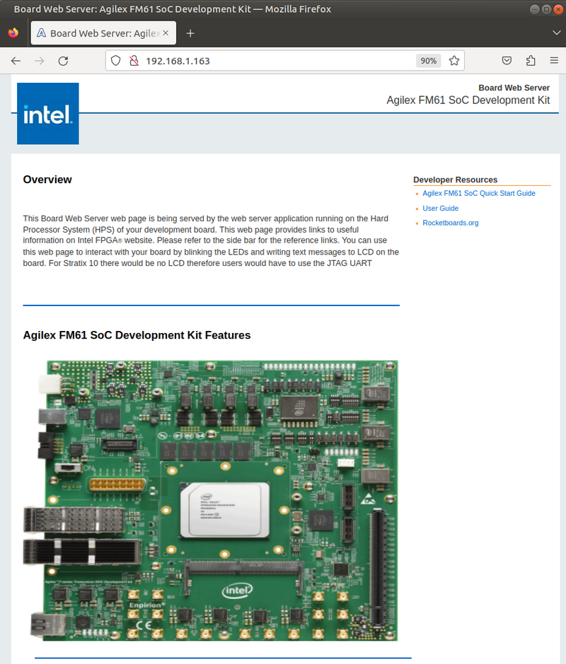
4. Scroll the webpage down to the section named Interacting with Agilex™ SoC Development Kit.
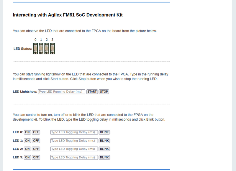
You will be able to perform the following actions:
- See which LEDs are ON and which are off in the LED Status. Note that if the LEDs are setup to be scrolling, the displayed scrolling speed will not match the actual scrolling speed on the board.
- Stop LEDs from scrolling, by clicking START and STOP buttons. The delay between LEDs turning ON and OFF is set in the LED Lightshow box.
- Turn individual LEDs ON and OFF with the ON and OFF buttons. Note that this action is only available when the LED scrolling/lightshow is stopped.
- Blink individual LEDs by typing a delay value in ms then clicking the corresponding BLINK button. Note that this action is only available when the LED scrolling/lightshow is stopped.
Connect With SSH
1. The lower bottom of the web page presents instructions on how to connect to the board using an SSH connection.
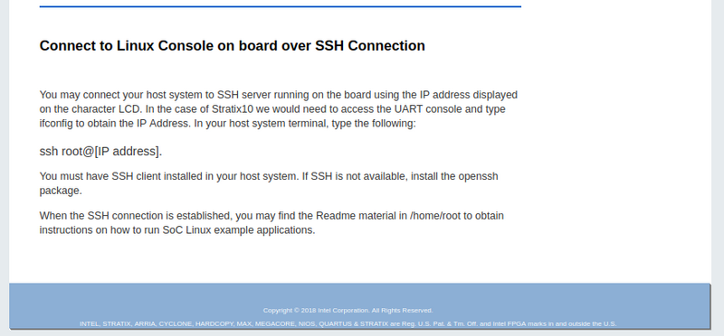
2. If the SSH client is not installed on your host computer, you can install it by running the following command on CentOS:
or the following command on Ubuntu:
3. Connect to the board, and run some commands, such as pwd, ls and uname to see Linux in action.
Boot from QSPI
Write QSPI Image
1. Download the QSPI image:
2. Configure MSEL to JTAG
3. Power cycle the board
4. Write the image using the following commands:
Boot Linux
1. Configure MSEL back to QSPI
2. Important: Remove SD card (or write zero to first few MBs) to confirm Linux is booting without it.
3. Power cycle. Board will boot up to Linux prompt, where you can login as 'root' without a password.
Note: First time Linux is booted, the UBIFS rootfs will be initialized, the step taking approximately 3 minutes, as shown in the log below:
[   12.272151] platform soc:leds: deferred probe pending
<-- ... 3 minute 'gap' here
[  216.905453] UBIFS (ubi0:4): free space fixup complete
[  217.035839] UBIFS (ubi0:4): UBIFS: mounted UBI device 0, volume 4, name "rootfs"
[  217.043228] UBIFS (ubi0:4): LEB size: 65408 bytes (63 KiB), min./max. I/O unit sizes: 8 bytes/256 bytes
[  217.052599] UBIFS (ubi0:4): FS size: 167117440 bytes (159 MiB, 2555 LEBs), max 6500 LEBs, journal size 8650240 bytes (8 MiB, 133 LEBs)
[  217.064650] UBIFS (ubi0:4): reserved for root: 0 bytes (0 KiB)
[  217.070469] UBIFS (ubi0:4): media format: w4/r0 (latest is w5/r0), UUID 4A5F6BFC-BA49-47C9-A17A-425E35F3A52F, small LPT model
[  217.271031] VFS: Mounted root (ubifs filesystem) on device 0:20
Boot from NAND
Write NAND Binaries
1. Download the files
wget https://releases.rocketboards.org/2026.10/nand/agilex7_dk_si_agf014eb_nand/qspi_helper.hps.jic
wget https://releases.rocketboards.org/2026.10/nand/agilex7_dk_si_agf014eb_nand/ghrd.hps.jic
wget https://releases.rocketboards.org/2026.10/nand/agilex7_dk_si_agf014eb_nand/u-boot.itb
wget https://releases.rocketboards.org/2026.10/nand/agilex7_dk_si_agf014eb_nand/root.ubi
2. Copy the binaries to your TFTP server:
3. Set MSEL to JTAG and power cycle. Then write qspi_helper.hps.jic to the QSPI:
4. Set MSEL to QSPI and power cycle.
5. Stop at U-Boot prompt, and run the following instructions to download and write NAND binaries to flash:
setenv autoload no
dhcp
setenv serverip <your-tftp-server-ip>

tftp $loadaddr u-boot.itb
nand erase.part u-boot
nand write $loadaddr u-boot $filesize

tftp $loadaddr root.ubi
nand erase.part clean root
nand write.trimffs $loadaddr root $filesize
Write QSPI Image
1. Power off board
2. Set MSEL to JTAG
3. Power on board
4. Write jic image to QSPI:
Boot Linux
1. Make sure board is powered off.
2. Set MSEL to QSPI
3. Power up the board.
4. Linux will boot, enter 'root' as user name to log in.
Boot From eMMC
This section presents how to exercise the boot from eMMC scenario for the System Example Design.
eMMC Daughtercard
The NAND/eMMC HPS daughtercard that comes with the DevKit supports both NAND and eMMC.
To configure the card for NAND operation, please set the jumpers as shown below:
| Jumper | Setting |
|---|---|
| J2 | unpopulated |
| J9 | unpopulated |
| J10 | populated 1-2 |
| J11 | populated 2-3 |
Write eMMC Image
The flow for writing the eMMC image is:
- Configure the FPGA over JTAG with the
baseline_hps_debug.soff - Load and run SPL and U-Boot to HPS over JTAG
- From U-Boot command prompt, transfer the eMMC image to HPS SDRAM over TFTP
- From U-Boot command prompt, write the eMMC image from SDRAM to eMMC
-
Run U-Boot from the debugger, as shown here https://altera-fpga.github.io/rel-25.3.1/embedded-designs/agilex-7/f-series/soc/boot-examples/ug-linux-boot-agx7-soc/#running-u-boot-with-the-debugger-from-command-line
-
The above will cause the U-Boot to start running on HPS. Stop U-Boot counter by pressing any key on the serial console.
-
Download, extract anhd split the eMMC image into 1GB chunks and copy them to your TFT folder:
Note: If using prebuilt binaries, extract first the wic image from
sdimage.tar.gz.
-
Determine the IP of your host computer running TFPT, by running 'ifconfig' command.
-
In U-Boot connect to the local network, and set the server ip parameter, where the tftp commands will connect to:
- In U-Boot, download the eMMC image and write it to flash:
tftp ${loadaddr} xaa
setexpr blkcnt1 ${filesize} / 0x200
mmc write ${loadaddr} 0 ${blkcnt1}
tftp ${loadaddr} xab
setexpr blkcnt2 ${filesize} / 0x200
mmc write ${loadaddr} ${blkcnt1} ${blkcnt2}
Write QSPI Image
1. Power off board
2. Set MSEL to JTAG
3. Power on board
4. Write jic image to QSPI:
Boot Linux
1. Make sure board is powered off.
2. Set MSEL to QSPI
3. Power up the board.
4. Linux will boot, enter 'root' as user name to log in.
Partial Reconfiguration
Partial reconfiguration (PR) allows you to reconfigure a portion of the FPGA dynamically, while the rest of the FPGA design continues to function. This section presents how to run the PR scenarios included with the System Example Design.
Quartus Design
The updated Quartus Design contains the following components which enable PR:
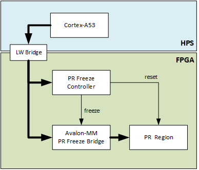
- A PR region was created in the FPGA fabric, with the following associated IP
- PR Freeze Controller - to help control the PR
- Avalon-MM PR Freeze Bridge - to help isolate the IP in the PR region during the PR process
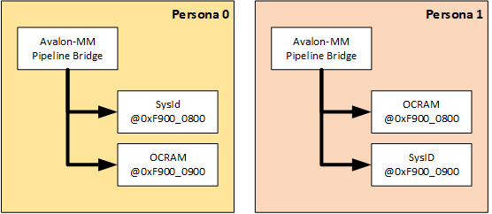
- The base revision of the project has the following in the PR region:
- SysID located at 0xF900_0800: with id=0xfacecafe
- OCRAM located at 0xF900_0900
- An alternate revision of the project contains the following in the PR region:
- SysID located at 0xF900_0900: with id=0xcafeface
- OCRAM located at 0xF900_0800
The following diagram presents an overview of the PR region and associated IP and how it is connected to HPS:
Throughout this page, the content of the PR region for the base revision is called "persona0" while the content of the PR region for the other revision is called "persona1". The diagram below illustrates the differences between the two personas:
PR Files
The files on the Linux rootfs used for running the PR scenarios are shown below:
| File | Description |
|---|---|
| /sbin/dtbt | Tool used for managing the overlays. Available at https://github.com/altera-opensource/dtbt |
| /boot/devicetree/agilex7_pr_fpga_static_region.dtbo | overlay for the static region, needs to be applied before persona overlays |
| /boot/devicetree/agilex7_pr_persona0.dtbo | overlay for persona0 |
| /boot/devicetree/agilex7_pr_persona0.dtbo | overlay for persona1 |
| /lib/firmware/persona0.rbf | bitstream used by persona0 overlay |
| /lib/firmware/persona1.rbf | bitstream used by persona1 overlay |
Run PR Scenarios
1. Boot Linux
2. Add the overlay for the static region:
root@agilex7dksiagf014eb:~# dtbt -a agilex7_pr_fpga_static_region.dtbo -p /boot/devicetree
Set dtbo search path to /boot/devicetree
[ 292.932872] OF: overlay: WARNING: memory leak will occur if overlay removed, property: /soc/base_fpga_region/ranges
Applying dtbo: agilex_pr_fpga_static_region.dtbo
[ 292.944184] OF: overlay: WARNING: memory leak will occur if overlay removed, property: /soc/base_fpga_region/external-fpga-config
[ 292.960109] OF: overlay: WARNING: memory leak will occur if overlay removed, property: /soc/base_fpga_region/clocks
[ 292.970529] OF: overlay: WARNING: memory leak will occur if overlay removed, property: /soc/base_fpga_region/clock-names
[ 292.981470] OF: overlay: WARNING: memory leak will occur if overlay removed, property: /__symbols__/clk_0
[ 292.991034] OF: overlay: WARNING: memory leak will occur if overlay removed, property: /__symbols__/freeze_controller_0
[ 293.007735] of-fpga-region soc:base_fpga_region:fpga_pr_region0: FPGA Region probed
[ 293.028076] altera_freeze_br f9000450.freeze_controller: fpga bridge [freeze] registered
3. Add the overlay for persona0:
root@agilex7dksiagf014eb:~# dtbt -a agilex7_pr_persona0.dtbo -p /boot/devicetree
Set dtbo search path to /boot/devicetree
[ 398.171799] fpga_manager fpga0: writing persona0.rbf to Stratix10 SOC FPGA Manager
Applying dtbo: agilex_pr_persona0.dtbo
[ 398.321356] OF: overlay: WARNING: memory leak will occur if overlay removed, property: /__symbols__/pr_region_0_pr_clk_100
[ 398.332459] OF: overlay: WARNING: memory leak will occur if overlay removed, property: /__symbols__/pr_region_0_pr_sysid_qsys_0
4. Locate the sysid and display the associated id:
root@agilex7dksiagf014eb:~# find / -name sysid
/sys/devices/platform/soc/soc:base_fpga_region/soc:base_fpga_region:fpga_pr_region0/f9000800.sysid/sysid
root@agilex7dksiagf014eb:~# cat /sys/devices/platform/soc/soc:base_fpga_region/soc:base_fpga_region:fpga_pr_region0/f9000800.sysid/sysid/id | xargs printf "0x%08x\n"
0xcafeface
5. List the applied overlays:
root@agilex7dksiagf014eb:~# dtbt -l
2 agilex_pr_persona0.dtbo applied /sys/kernel/config/device-tree/overlays/2-agilex_pr_persona0.dtbo
1 agilex_pr_fpga_static_region.dtbo applied /sys/kernel/config/device-tree/overlays/1-agilex_pr_fpga_static_region.dtbo
6. Remove persona0 overlay:
root@agilex7dksiagf014eb:~# dtbt -r agilex7_pr_persona0.dtbo -p /boot/devicetree
Set dtbo search path to /boot/devicetree
Removing dtbo: 2-agilex_pr_persona0.dtbo
7. Add the persona1 overlay:
root@agilex7dksiagf014eb:~# dtbt -a agilex7_pr_persona1.dtbo -p /boot/devicetree
Set dtbo search path to /boot/devicetree
[ 531.975623] fpga_manager fpga0: writing persona1.rbf to Stratix10 SOC FPGA Manager
Applying dtbo: agilex_pr_persona1.dtbo
[ 532.124433] OF: overlay: WARNING: memory leak will occur if overlay removed, property: /__symbols__/pr_region_0_pr_clk_100
[ 532.135530] OF: overlay: WARNING: memory leak will occur if overlay removed, property: /__symbols__/pr_region_0_pr_sysid_qsys_0
8. Locate the sysid and display the associated id:
root@agilex7dksiagf014eb:~# find / -name sysid
/sys/devices/platform/soc/soc:base_fpga_region/soc:base_fpga_region:fpga_pr_region0/f9000900.sysid/sysid
root@agilex7dksiagf014eb:~# cat /sys/devices/platform/soc/soc:base_fpga_region/soc:base_fpga_region:fpga_pr_region0/f9000900.sysid/sysid/id | xargs printf "0x%08x\n"
0xfacecafe
9. Remove persona1:
root@agilex7dksiagf014eb:~# dtbt -r agilex7_pr_persona1.dtbo -p /boot/devicetree
Set dtbo search path to /boot/devicetree
Removing dtbo: 2-agilex_pr_persona1.dtbo
10. List the applied overlays:
root@agilex7dksiagf014eb:~# dtbt -l
1 agilex_pr_fpga_static_region.dtbo applied /sys/kernel/config/device-tree/overlays/1-agilex_pr_fpga_static_region.dtbo
Rebuild Binaries
The embedded software for this System Example Design is built with Yocto, using KAS.
Kas is a Python-based lightweight build orchestration layer on top of BitBake/Yocto. Kas allows you to define your build environment in a YAML manifest, so you can perform checkout, environment setup, configuration, and build invocation with a single command. Kas provides a more maintainable build description, it offers improved reproducibility, reduced setup friction, and a clearer abstraction for managing multiple layers, revisions, and configuration fragments.
The software source code for this System Example Design is released inside the software/yocto_linux directory. Accessing the link will display a README page with details regarding the software.
For more details about Kas, refer to the official documentation at https://kas.readthedocs.io/en/latest/.
Kas Build Prerequisites
Firtst, the same prerequisites as for regular Yocto build are required.
1. Make sure you have Yocto system requirements met: https://docs.yoctoproject.org/scarthgap/ref-manual/system-requirements.html#supported-linux-distributions.
The command to install the required packages on Ubuntu 22.04 is:
sudo apt-get update
sudo apt-get upgrade
sudo apt-get install openssh-server mc libgmp3-dev libmpc-dev gawk wget git diffstat unzip texinfo gcc \
build-essential chrpath socat cpio python3 python3-pip python3-pexpect xz-utils debianutils iputils-ping \
python3-git python3-jinja2 libegl1-mesa libsdl1.2-dev pylint xterm python3-subunit mesa-common-dev zstd \
liblz4-tool git fakeroot build-essential ncurses-dev xz-utils libssl-dev bc flex libelf-dev bison xinetd \
tftpd tftp nfs-kernel-server libncurses5 libc6-i386 libstdc++6:i386 libgcc++1:i386 lib32z1 \
device-tree-compiler curl mtd-utils u-boot-tools net-tools swig -y
On Ubuntu 22.04 you will also need to point the /bin/sh to /bin/bash, as the default is a link to /bin/dash:
Note: You can also use a Docker container to build the Yocto recipes, refer to https://rocketboards.org/foswiki/Documentation/DockerYoctoBuild for details. When using a Docker container, it does not matter what Linux distribution or packages you have installed on your host, as all dependencies are provided by the Docker container.
In addition to the above, you must also install python3-newt, and python3.10-venv with a command like this:
Boot from SD Card
Build Flow
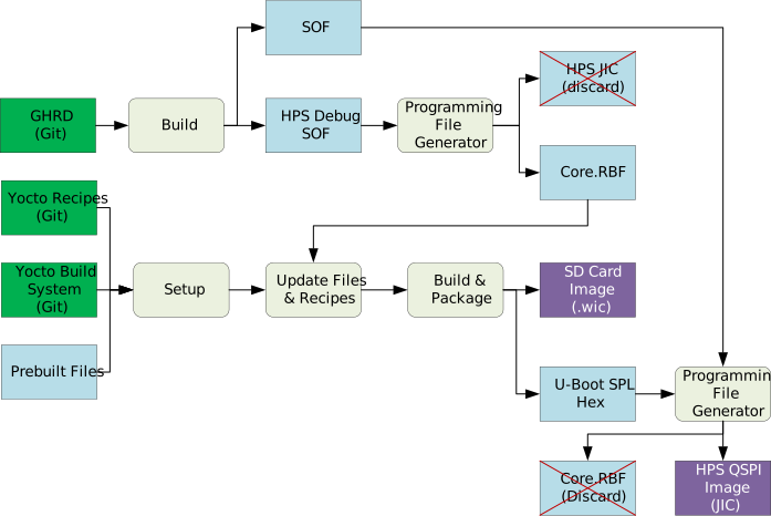
The following diagram illustrates the full build flow for the System Example Design, based on source code from GitHub.
Set up Environment
Create a top folder for this example, as the rest of the commands assume this location:
Enable Quartus tools to be called from command line:
Build Quartus Design
Use the following commands to build the Quartus Design:
cd $TOP_FOLDER
rm -rf dk-si-agf014eb-oobe-baseline
mkdir dk-si-agf014eb-oobe-baseline
cd dk-si-agf014eb-oobe-baseline
wget https://github.com/altera-fpga/agilex7-ed-hps-baseline/releases/download/QPDS26.3_REL_BASELINE_PR/dk-si-agf014eb-oobe-baseline.zip
unzip dk-si-agf014eb-oobe-baseline.zip
rm -f dk-si-agf014eb-oobe-baseline.zip
make baseline-install
The following files are created:
$TOP_FOLDER/dk-si-agf014eb-oobe-baseline/install/binaries/baseline.sof- FPGA configuration file, without HPS FSBL$TOP_FOLDER/dk-si-agf014eb-oobe-baseline/install/binaries/ghrd.core.rbf- FPGA fabric configuration file
Build Yocto Using Kas
1. Create and enter a new Python virtual environment:
cd $TOP_FOLDER/dk-si-agf014eb-oobe-baseline/software/yocto_linux
python3 -m venv venv --system-site-packages
source venv/bin/activate
pip install --upgrade pip
pip install kas
pip install --upgrade kas
pip install kconfiglib
2. Copy the core.rbf file to where Kas expects it to be:
cp $TOP_FOLDER/dk-si-agf014eb-oobe-baseline/install/binaries/ghrd.core.rbf meta-custom/recipes-fpga/fpga-bitstream/files/baseline_hps_debug.core.rbf
3. Build Yocto with Kas:
The following relevant files are created in $TOP_FOLDER/dk-si-agf014eb-oobe-baseline/software/yocto_linux/build/tmp/deploy/images/agilex7/:
gsrd-console-image-agilex7.rootfs.wicconsole-image-minimal-agilex7.rootfs_nor.ubifsu-boot-spl-dtb.hex
Note: If you experience build failures related to file-locks, you can work around these by reducing the parallelism of your build by running the following commands before running
kas:
export PARALLEL_MAKE="-j 8"
export BB_NUMBER_THREADS="8"
export BB_ENV_PASSTHROUGH_ADDITIONS="$BB_ENV_PASSTHROUGH_ADDITIONS PARALLEL_MAKE BB_NUMBER_THREADS"
Create QSPI Image
The QSPI image will contain the FPGA configuration data and the HPS FSBL and it can be built using the following command:
cd $TOP_FOLDER
rm -f *jic* *rbf*
quartus_pfg -c $TOP_FOLDER/dk-si-agf014eb-oobe-baseline/install/binaries/baseline.sof \
 ghrd.jic \
 -o hps_path=$TOP_FOLDER/dk-si-agf014eb-oobe-baseline/software/yocto_linux/build/tmp/deploy/images/agilex7/u-boot-spl-dtb.hex \
 -o device=MT25QU02G \
 -o flash_loader=AGFB014R24B2E2V \
 -o mode=ASX4 \
 -o hps=1
The following files will be created:
- $TOP_FOLDER/ghrd.hps.jic - Flash image for HPS First configuration bitstream, phase 1: HPS and DDR
- $TOP_FOLDER/ghrd.core.rbf - HPS First configuration bitstream, phase 2: FPGA fabric, discarded, as we already have it on the SD card
Boot from QSPI
This section presents how to boot from QSPI.
Much of the same binaries as when booting from SD card can be used to boot from QSPI, because:
- The QSPI resides on the DevKit board, and not on the HPS daughtercard, so there are no board changes:
- The same Quartus Design configuration can be used
- The same U-Boot devce tree can be used
- The same Linux device tree can be used
- U-Boot uses distroboot, which will try first booting from SD/MMC, then from QSPI, then from NAND, so the same U-Boot can be used.
As the QSPI has a much smaller size than the SD card (256MB vs 2GB) the rootfs is smaller, and less functionality is provided. The purpose of this section is just to show Linux booting.
Note: The HPS speed for accessing SDM QSPI is limited to ~8MB/s. It is up to you to decide whether this level of performance is sufficient for your application. If not, it is recommended you use an SD card or eMMC device to store the HPS components such as the rootfs. Note that the QSPI speed limitation does not apply when SDM accesses the QSPI, it is just for HPS accessing SDM QSPI.
QSPI Flash Layout
| MTD Partition | UBI Volume | Volume Name | Type | Image/Individual File | Group File | Size |
|---|---|---|---|---|---|---|
| 0 (qspi_uboot) | N/A N/A |
N/A N/A |
RAW RAW |
bitstream (FPGA image, SDM firmware) u-boot.itb |
N/A N/A |
64MB 2MB |
| 1 (qspi_root) | 0 1 2 3 4 |
env script kernel dtb rootfs |
UBI UBI UBI UBI UBIFS |
u-boot.env u-boot.scr kernel.itb kernel.dtb rootfs.ubifs |
root.ubi |
256KB 128KB 24MB 256KB 160MB |
Create QSPI Image
1. Create a folder to contain all the qspi binaries, and create symlinks to actual location for all files:
cd $TOP_FOLDER
rm -rf qspi-boot && mkdir qspi-boot && cd qspi-boot
ln -s $TOP_FOLDER/dk-si-agf014eb-oobe-baseline/install/binaries/baseline.sof ghrd.sof
ln -s $TOP_FOLDER/dk-si-agf014eb-oobe-baseline/software/yocto_linux/build/tmp/deploy/images/agilex7/u-boot.itb u-boot.bin
ln -s $TOP_FOLDER/dk-si-agf014eb-oobe-baseline/software/yocto_linux/build/tmp/deploy/images/agilex7/u-boot-spl-dtb.hex .
ln -s $TOP_FOLDER/dk-si-agf014eb-oobe-baseline/software/yocto_linux/build/tmp/deploy/images/agilex7/boot.scr.uimg .
ln -s $TOP_FOLDER/dk-si-agf014eb-oobe-baseline/software/yocto_linux/build/tmp/deploy/images/agilex7/kernel.itb .
ln -s $TOP_FOLDER/dk-si-agf014eb-oobe-baseline/software/yocto_linux/build/tmp/deploy/images/agilex7/uboot.env .
ln -s $TOP_FOLDER/dk-si-agf014eb-oobe-baseline/software/yocto_linux/build/tmp/deploy/images/agilex7/console-image-minimal-agilex7.rootfs_nor.ubifs .
2. Create hps.ubi file:
cd $TOP_FOLDER/qspi-boot
wget https://releases.rocketboards.org/2026.10/qspi/agilex7_dk_si_agf014eb_qspi/ubinize_nor.cfg
ubinize -o root.ubi -p 65536 -m 1 -s 1 ubinize_nor.cfg
ln -s root.ubi hps.bin
3. Create the QSPI image using the provided Quartus Programming File Generator (PFG) file:
cd $TOP_FOLDER/qspi-boot
wget https://releases.rocketboards.org/2026.10/qspi/agilex7_dk_si_agf014eb_qspi/qspi_boot.pfg
quartus_pfg -c qspi_boot.pfg
This will create the following file:
$TOP_FOLDER/qspi-boot/qspi_boot.hps.jic
Boot From NAND
This section presents how to boot from NAND, including how to build all binaries.
Build instructions are the same as for standard SD or QSPI boot. The U-Boot, ATF and Linux binaries are all the same. The only difference is that the Quartus Design is configured for the NAND HPS Daughtercard, then recompiled.
Note: As the NAND used on the devkit has a smaller size than the SD card (1GB vs 2GB) the rootfs is smaller, and less functionality is provided. The purpose of this section is just to show Linux booting.
NAND Flash Layout
| MTD Partition | UBI Volume | Volume Name | Type | Image/File | Flash Offset | Size | Size in Hex | |
|---|---|---|---|---|---|---|---|---|
| 0 (u-boot) | N/A | N/A | RAW | u-boot.itb | 0x00000000 | 2MB | 0x00200000 | |
| 1 (root) | 0 | env | UBI | u-boot.env | root.ubi | 0x00200000 onwards | 256KB | 0x40000 |
| 1 | script | UBI | u-boot.scr | 128KB | 0x00020000 | |||
| 2 | kernel | UBI | kernel.itb | 64MB | 0x04000000 | |||
| 3 | dtb | UBI | kernel.dtb | 256KB | 0x00040000 | |||
| 4 | rootfs | UBIFS | rootfs.ubifs | <957MB | <0x3BD70000 |
Set up Environment
Create a top folder for this example, as the rest of the commands assume this location:
sudo rm -rf agilex7f_baseline.nand
mkdir agilex7f_baseline.nand
cd agilex7f_baseline.nand
export TOP_FOLDER=$(pwd)
Enable Quartus tools to be called from command line:
Build Quartus Design
Use the following commands to build the hardware design:
cd $TOP_FOLDER
rm -rf dk-si-agf014eb-nand-baseline
mkdir dk-si-agf014eb-nand-baseline
cd dk-si-agf014eb-nand-baseline
wget https://github.com/altera-fpga/agilex7-ed-hps-baseline/releases/download/QPDS26.3_REL_BASELINE_PR/dk-si-agf014eb-nand-baseline.zip
unzip dk-si-agf014eb-nand-baseline.zip
rm -f dk-si-agf014eb-nand-baseline.zip
make baseline-install
The following files are created:
$TOP_FOLDER/dk-si-agf014eb-nand-baseline/install/binaries/baseline.sof- FPGA configuration file, without HPS FSBL$TOP_FOLDER/dk-si-agf014eb-nand-baseline/install/binaries/ghrd.core.rbf- FPGA fabric configuration file
Build Yocto Using Kas
1. Create and enter a new Python virtual environment:
cd $TOP_FOLDER/dk-si-agf014eb-nand-baseline/software/yocto_linux
python3 -m venv venv --system-site-packages
source venv/bin/activate
pip install --upgrade pip
pip install kas
pip install --upgrade kas
pip install kconfiglib
2. Copy the core.rbf file to where Kas expects it to be:
cp $TOP_FOLDER/dk-si-agf014eb-nand-baseline/install/binaries/ghrd.core.rbf meta-custom/recipes-fpga/fpga-bitstream/files/baseline_hps_debug.core.rbf
3. Build Yocto with Kas:
The following relevant files are created in $TOP_FOLDER/dk-si-agf014eb-nand-baseline/software/yocto_linux/build/tmp/deploy/images/agilex7/:
console-image-minimal-agilex7.rootfs_nand.ubifsu-boot-spl-dtb.hex
Note: If you experience build failures related to file-locks, you can work around these by reducing the parallelism of your build by running the following commands before running
kas:
export PARALLEL_MAKE="-j 8"
export BB_NUMBER_THREADS="8"
export BB_ENV_PASSTHROUGH_ADDITIONS="$BB_ENV_PASSTHROUGH_ADDITIONS PARALLEL_MAKE BB_NUMBER_THREADS"
Create QSPI Image
The QSPI image will contain the FPGA configuration data and the HPS FSBL and it can be built using the following command:
cd $TOP_FOLDER
rm -f *jic* *rbf*
quartus_pfg -c $TOP_FOLDER/dk-si-agf014eb-nand-baseline/install/binaries/baseline.sof \
 ghrd.jic \
 -o hps_path=$TOP_FOLDER/dk-si-agf014eb-nand-baseline/software/yocto_linux/build/tmp/deploy/images/agilex7/u-boot-spl-dtb.hex \
 -o device=MT25QU02G \
 -o flash_loader=AGFB014R24B2E2V \
 -o mode=ASX4 \
 -o hps=1
The following files will be created:
$TOP_FOLDER/ghrd.hps.jic- Flash image for HPS First configuration bitstream, phase 1: HPS and DDR$TOP_FOLDER/ghrd.core.rbf- HPS First configuration bitstream, phase 2: FPGA fabric, discarded, as we already have it on the SD card
Build NAND Binaries
1. Gather the files into a single folder, using symlinks:
cd $TOP_FOLDER
rm -rf nand-bin && mkdir nand-bin && cd nand-bin
ln -s $TOP_FOLDER/dk-si-agf014eb-nand-baseline/software/yocto_linux/build/tmp/deploy/images/agilex7/uboot.env .
ln -s $TOP_FOLDER/dk-si-agf014eb-nand-baseline/software/yocto_linux/build/tmp/deploy/images/agilex7/boot.scr.uimg .
ln -s $TOP_FOLDER/dk-si-agf014eb-nand-baseline/software/yocto_linux/build/tmp/deploy/images/agilex7/kernel.itb .
ln -s $TOP_FOLDER/dk-si-agf014eb-nand-baseline/software/yocto_linux/build/tmp/deploy/images/agilex7/console-image-minimal-agilex7.rootfs_nand.ubifs .
2. Install mtd-tools if not already installed. On Ubuntu the command is:
3. Create UBI configuration file for the root partition:
4. Create the root.ubi file:
This is what the above parameters mean:
- -p: physical eraseblock size of the flash
- -m: minimum input/output unit size of the flash
- -s: sub-pages and sub-page size, ubinize will take into account and put the VID header to same NAND page as the EC header
The following file is created:
- $TOP_FOLDER/nand-bin/root.ubi
Boot from eMMC
Build Flow
The following diagram illustrates the full build flow for the System Example Design, based on source code from GitHub.
Set up Environment
Create a top folder for this example, as the rest of the commands assume this location:
sudo rm -rf agilex7f_baseline.emmc
mkdir agilex7f_baseline.emmc
cd agilex7f_baseline.emmc
export TOP_FOLDER=$(pwd)
Enable Quartus tools to be called from command line:
Build Quartus Design
Use the following commands to build the Quartus Design:
cd $TOP_FOLDER
rm -rf dk-si-agf014eb-emmc-baseline
mkdir dk-si-agf014eb-emmc-baseline
cd dk-si-agf014eb-emmc-baseline
wget https://github.com/altera-fpga/agilex7-ed-hps-baseline/releases/download/QPDS26.3_REL_BASELINE_PR/dk-si-agf014eb-emmc-baseline.zip
unzip dk-si-agf014eb-emmc-baseline.zip
rm -f dk-si-agf014eb-emmc-baseline.zip
make baseline-install
The following files are created:
$TOP_FOLDER/dk-si-agf014eb-emmc-baseline/install/binaries/baseline.sof- FPGA configuration file, without HPS FSBL$TOP_FOLDER/dk-si-agf014eb-emmc-baseline/install/binaries/ghrd.core.rbf- FPGA fabric configuration file
Build Yocto Using Kas
1. Create and enter a new Python virtual environment:
cd $TOP_FOLDER/dk-si-agf014eb-emmc-baseline/software/yocto_linux
python3 -m venv venv --system-site-packages
source venv/bin/activate
pip install --upgrade pip
pip install kas
pip install --upgrade kas
pip install kconfiglib
2. Copy the core.rbf file to where Kas expects it to be:
cp $TOP_FOLDER/dk-si-agf014eb-emmc-baseline/install/binaries/ghrd.core.rbf meta-custom/recipes-fpga/fpga-bitstream/files/baseline_hps_debug.core.rbf
3. Build Yocto with Kas:
The following relevant files are created in $TOP_FOLDER/dk-si-agf014eb-emmc-baseline/software/yocto_linux/build/tmp/deploy/images/agilex7/:
gsrd-console-image-agilex7.rootfs.wicu-boot-spl-dtb.hex
Note: If you experience build failures related to file-locks, you can work around these by reducing the parallelism of your build by running the following commands before running
kas:
export PARALLEL_MAKE="-j 8"
export BB_NUMBER_THREADS="8"
export BB_ENV_PASSTHROUGH_ADDITIONS="$BB_ENV_PASSTHROUGH_ADDITIONS PARALLEL_MAKE BB_NUMBER_THREADS"
Create QSPI Image
The QSPI image will contain the FPGA configuration data and the HPS FSBL and it can be built using the following command:
cd $TOP_FOLDER
rm -f *jic* *rbf*
quartus_pfg -c  $TOP_FOLDER/dk-si-agf014eb-emmc-baseline/install/binaries/baseline.sof \
 ghrd.jic \
 -o hps_path=$TOP_FOLDER/dk-si-agf014eb-emmc-baseline/software/yocto_linux/build/tmp/deploy/images/agilex7/u-boot-spl-dtb.hex \
 -o device=MT25QU02G \
 -o flash_loader=AGFB014R24B2E2V \
 -o mode=ASX4 \
 -o hps=1
The following files will be created:
- $TOP_FOLDER/ghrd.hps.jic - Flash image for HPS First configuration bitstream, phase 1: HPS and DDR
- $TOP_FOLDER/ghrd.core.rbf - HPS First configuration bitstream, phase 2: FPGA fabric, discarded, as we already have it on the SD card
Partial Reconfiguration
Partial reconfiguration (PR) allows you to reconfigure a portion of the FPGA dynamically, while the rest of the FPGA design continues to function.
This section shows how to build everything needed to demonstrate the PR scenarios. Note that most of the binaries are the same as for the other boot scenarios (SD card, QSPI, NAND) just the following files are changed:
- New Quartus Design variant, creating different configuration bitstreams
- Updated core.rbf, persona0.rbf, persona1.rbf compared to prebuilt default files used by the Yocto recipes
Set up Environment
Create a top folder for this example, as the rest of the commands assume this location:
Enable Quartus tools to be called from command line:
Build Quartus Design
Use the following commands to build the Quartus Design:
cd $TOP_FOLDER
rm -rf dk-si-agf014eb-oobe-pr
mkdir dk-si-agf014eb-oobe-pr
cd dk-si-agf014eb-oobe-pr
wget https://github.com/altera-fpga/agilex7-ed-hps-baseline/releases/download/QPDS26.3_REL_BASELINE_PR/dk-si-agf014eb-oobe-pr.zip
unzip dk-si-agf014eb-oobe-pr.zip
rm -f dk-si-agf014eb-oobe-pr.zip
make pr-install alternate_persona-install
The following files are created:
$TOP_FOLDER/dk-si-agf014eb-oobe-pr/install/binaries/pr.sof$TOP_FOLDER/dk-si-agf014eb-oobe-pr/install/binaries/ghrd.core.rbf$TOP_FOLDER/dk-si-agf014eb-oobe-pr/install/binaries/dk-si-agf014eb-oobe_pr_persona0.rbf$TOP_FOLDER/dk-si-agf014eb-oobe-pr/install/binaries/dk-si-agf014eb-oobe_pr_persona1.rbf
Build Yocto Using Kas
1. Create and enter a new Python virtual environment:
cd $TOP_FOLDER/dk-si-agf014eb-oobe-pr/software/yocto_linux
python3 -m venv venv --system-site-packages
source venv/bin/activate
pip install --upgrade pip
pip install kas
pip install --upgrade kas
pip install kconfiglib
2. Copy the core.rbf file to where Kas expects it to be:
cp $TOP_FOLDER/dk-si-agf014eb-oobe-pr/install/binaries/ghrd.core.rbf meta-custom/recipes-fpga/fpga-bitstream/files/pr_hps_debug.core.rbf
cp $TOP_FOLDER/dk-si-agf014eb-oobe-pr/install/binaries/dk-si-agf014eb-oobe_pr_persona0.rbf meta-custom/recipes-fpga/fpga-bitstream/files/persona0.rbf
cp $TOP_FOLDER/dk-si-agf014eb-oobe-pr/install/binaries/dk-si-agf014eb-oobe_pr_persona1.rbf meta-custom/recipes-fpga/fpga-bitstream/files/persona1.rbf
3. Build Yocto with Kas:
The following relevant files are created in $TOP_FOLDER/dk-si-agf014eb-oobe-pr/software/yocto_linux/build/tmp/deploy/images/agilex7/:
gsrd-console-image-agilex7.rootfs.wicu-boot-spl-dtb.hex
Note: If you experience build failures related to file-locks, you can work around these by reducing the parallelism of your build by running the following commands before running
kas:
export PARALLEL_MAKE="-j 8"
export BB_NUMBER_THREADS="8"
export BB_ENV_PASSTHROUGH_ADDITIONS="$BB_ENV_PASSTHROUGH_ADDITIONS PARALLEL_MAKE BB_NUMBER_THREADS"
Create QSPI Image
The QSPI image will contain the FPGA configuration data and the HPS FSBL and it can be built using the following command:
cd $TOP_FOLDER
rm -f *jic* *rbf*
quartus_pfg -c $TOP_FOLDER/dk-si-agf014eb-oobe-pr/install/binaries/pr.sof \
 ghrd.jic \
 -o hps_path=$TOP_FOLDER/dk-si-agf014eb-oobe-pr/software/yocto_linux/build/tmp/deploy/images/agilex7/u-boot-spl-dtb.hex \
 -o device=MT25QU02G \
 -o flash_loader=AGFB014R24B2E2V \
 -o mode=ASX4 \
 -o hps=1
The following files will be created:
- $TOP_FOLDER/ghrd.hps.jic - Flash image for HPS First configuration bitstream, phase 1: HPS and DDR
- $TOP_FOLDER/ghrd.core.rbf - HPS First configuration bitstream, phase 2: FPGA fabric, discarded, as we already have it on the SD card
How to Manually Update the kernel.itb file
The kernel.itb file is a Flattattened Image Tree (FIT) file that includes the following components:
- Linux kernel.
- Board configurations* that indicate what components from the kernel.itb (Linux kernel, device tree and Phase 2 FPGA configuration bitstream) should be used for a specific board.
- Linux device tree*.
- Phase 2 FPGA configuration bitstream*.
* One or more of these components to support the different board configurations.
The kernel.itb is created from a .its (Image Tree Source file) that describes its structure. In the HPS Baseline System Example Design, the kernel.itb file is generated in the following directory. In this directory you can also find the .its files and all other the components needed to create the kernel.itb :
- $TOP_FOLDER/<gsrd-directory>/<project-directory>/software/yocto_linux/build/tmp*/work/<device>-poky-linux/linux-socfpga-lts/<linux-branch>+git/linux-<device>-standard-build/
As an example of this path, for the Agilex 5 device you will find this directory as $TOP_FOLDER/a5ed065es-premium-devkit-oobe/baseline-a55/software/yocto_linux/build/tmp*/work/agilex5e-poky-linux/linux-socfpga-lts/6.12.43-lts+git/linux-agilex5e-standard-build
If you want to modify the kernel.itb by replacing one of the component or modifying any board configuration, you can do the following:
-
Install mtools package in your Linux machine.
-
Go to the folder in which the kernel.itb is being created under the HPS Baseline System Example Design.
-
In the .its file, observe the components that integrates the kernel.itb identifying the nodes as indicated next:
images node:
- kernel node - Linux kernel defined with the data parameter in the node.
- fdt-X node - Device tree X defined with the data parameter in the node.
- fpga-X node - Phase 2 FPGA configuration bitstream .rbf defined with the data parameter in the node.configurations node:
- board-X node - Board configuration with the name defined with the description parameter. The components for a specific board configuration are defined with the kernel, fdt and fpga parameters. -
In this directory, you can replace any of the file components that integrate the kernel.itb, or you can also modify the .its to change the structure and components of the kernel.itb.
-
Finally, you need to re-generate the new kernel.itb running the following command in the same linux-
-standard-build/ directory.
Once that you have completed this procedure, you can use the new kernel.itb as needed. Some options could be:
- Use U-Boot to load this into the SDRAM board through TFTP to boot Linux or to write it to a flash device
- Directly update the flash image in your board (QSPI, SD Card, eMMC or NAND) from your working machine.
How to Manually Update the SD Card Content file
As part of the Yocto HPS Baseline System Example Designbuild flow, the SD Card image is built for the SD Card boot flow. This image includes a couple of partitions. One of these partition (a FAT32) includes the U-Boot proper, the Distroboot boot script, U-Boot environment and the Linux .itb - which includes the Linux kernel image, the Linux device tree, the phase 2 FPGA configuration bitstream and board configuration (there may be several versions of these last 3 components). The 2nd partition (an EXT3 or EXT4 ) includes the Linux file system.
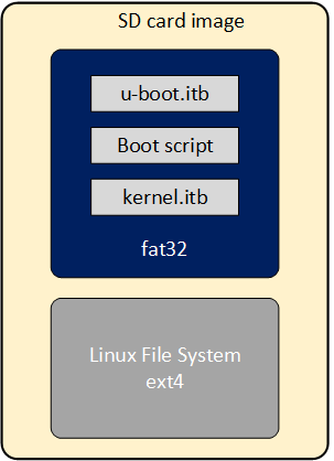
If you want to replace any the components or add a new item in any of these partitions, without having to run again the Yocto build flow.
This can be done through the wic script available on the Poky repository that is included as part of the HPS Baseline System Example Design build directory:
- $TOP_FOLDER/<gsrd-directory>/<project-directory>/software/yocto_linux/poky/scripts/wic
The wic command requires to be run in the Yocto build environment that can be setup as shown next in a Linux terminal:
cd $TOP_FOLDER/<gsrd-directory>/<project-directory>/software/yocto_linux/
source poky/oe-init-build-env build
The wic command allows you to inspect the content of a SD Card image, delete, add or replace any component inside of the image. This command is also provided with help support:
$ $TOP_FOLDER/<gsrd-directory>/<project-directory>/software/yocto_linux/poky/scripts/wic help

Creates a customized OpenEmbedded image.

Usage:  wic [--version]
        wic help [COMMAND or TOPIC]
        wic COMMAND [ARGS]

    usage 1: Returns the current version of Wic
    usage 2: Returns detailed help for a COMMAND or TOPIC
    usage 3: Executes COMMAND

COMMAND:

 list   -   List available canned images and source plugins
 ls     -   List contents of partitioned image or partition
 rm     -   Remove files or directories from the vfat or ext* partitions
 help   -   Show help for a wic COMMAND or TOPIC
 write  -   Write an image to a device
 cp     -   Copy files and directories to the vfat or ext* partitions
 create -   Create a new OpenEmbedded image
 :
 :
The following steps show you how to replace the kernel.itb file inside of the fat32 partition in a .wic image.
-
The wic ls command allows you to inspect or navigate over the directory structure inside of the SD Card image. For example you can observe the partitions in the SD Card image in this way.
# Here you can inspect the content a wic image see the 2 partitions inside of the SD Card image $ $TOP_FOLDER/<gsrd-directory>/<project-directory>/software/yocto_linux/poky/scripts/wic ls my_image.wic Num Start End Size Fstype 1 1048576 525336575 524288000 fat32 2 525336576 2098200575 1572864000 ext4 # Here you can naviagate inside of the partition 1 $ $TOP_FOLDER/<gsrd-directory>/<project-directory>/software/yocto_linux/poky/scripts/wic ls my_image.wic:1 Volume in drive : is boot Volume Serial Number is 8F65-ACE9 Directory for ::/ BOOTSC~1 UIM 2739 2011-04-05 23:00 boot.scr.uimg kernel itb 12885831 2011-04-05 23:00 uboot env 8192 2011-04-05 23:00 u-boot itb 938816 2011-04-05 23:00 4 files 13 835 578 bytes 509 370 368 bytes free -
The wic rm command allows you to delete any of the components in the selected partition. For example, you can delete the kernel.itb image from the partition 1(fat32 partition).
-
The wic cp command allows you to copy any new item or file from your Linux machine to a specific partition and location inside of the SD Card image. For example, you can copy a new kernel.itb to the partition 1.
NOTE: The wic application also allows you to modify any image with compatible vfat and ext* type partitions which also covers images used for eMMC boot flow.
Notices & Disclaimers
Altera® Corporation technologies may require enabled hardware, software or service activation. No product or component can be absolutely secure. Performance varies by use, configuration and other factors. Your costs and results may vary. You may not use or facilitate the use of this document in connection with any infringement or other legal analysis concerning Altera or Intel products described herein. You agree to grant Altera Corporation a non-exclusive, royalty-free license to any patent claim thereafter drafted which includes subject matter disclosed herein. No license (express or implied, by estoppel or otherwise) to any intellectual property rights is granted by this document, with the sole exception that you may publish an unmodified copy. You may create software implementations based on this document and in compliance with the foregoing that are intended to execute on the Altera or Intel product(s) referenced in this document. No rights are granted to create modifications or derivatives of this document. The products described may contain design defects or errors known as errata which may cause the product to deviate from published specifications. Current characterized errata are available on request. Altera disclaims all express and implied warranties, including without limitation, the implied warranties of merchantability, fitness for a particular purpose, and non-infringement, as well as any warranty arising from course of performance, course of dealing, or usage in trade. You are responsible for safety of the overall system, including compliance with applicable safety-related requirements or standards. © Altera Corporation. Altera, the Altera logo, and other Altera marks are trademarks of Altera Corporation. Other names and brands may be claimed as the property of others.
OpenCL* and the OpenCL* logo are trademarks of Apple Inc. used by permission of the Khronos Group™.