Setting up and Using Bridges HPS Linux Example
Overview
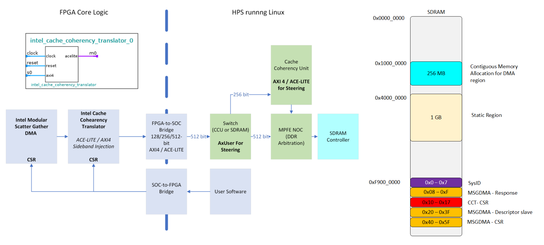
This project demonstrates how to access HPS Memory via the FPGA to HPS bridges when the HPS is running Linux, but is also applicable to other OS’s or BareMetal inclusive. This project is created for the Agilex™ 7 FPGA F-Series Transceiver-SoC Development Kit (P-Tiles & E-Tile, DK-SI-AGF014EB). It includes the effect of:
- The memory allocation method used in Linux which sets the memory attributes including security and privilege.
- The interaction with Arm® AMBA® AXI™ Side Band Signal settings required for secure, privileged, and cached transfers from the FPGA using the Cache Coherency Translator IP. This also includes the exercise of the data path that goes from fabric to SDRAM which could go directly to SDRAM or pass through CCU.
- The Firewall settings for the HPS bridges, which can override AXI transaction attributes.
- Perform data movement from one SDRAM memory location to another using the Scatter-Gather DMA IP.
This example allocates memory using two methods:
-
Manually reserved memory at Kernel boot time.
- Allocation at Kernel boot time using the Kernel boot argument mem=1G. This limits the Linux kernel to use the lower 1GB (of 2 GB*) SDRAM.
- This creates a static area of 1 GB (upper region of the 2 GB*) reserved for the application.
- This area will typically be marked as Privileged and non-secure, but this is implementation dependent.
-
Runtime allocation from the Contiguous Memory Allocator Area (CMA) of 256 MB.
- Kernel allocated memory from device tree supported by Kernel drivers, dynamic allocation of DMA Memory and the Linux Kernel’s DMA API.
- An open source 3rd party driver is used to allocate this memory.
- This memory will typically be marked as privileged as it has been kernel allocated, and may be marked as non-secure.
Note: The dev kit have 8 GB of memory which is mapped in 2 regions: one region of 2 GB (going from 0x0 - 0x80000000) and second region of 6 GB (going from 0x280000000 - 0x400000000). The 2 GB region mentioned in the manually reserved memory above is referring to this 1st region.
For further reading:
- Linux Kernel DMA API, and CMA documentation can be found in the Linux Kernel Documentation.
- Information on Memory Attributes in Arm® architectures can be found in the Arm Architecture documentation available on arm.com.
This example requires a correct configuration for the FPGA Firewall settings to allow only secure access through F2S bridge( through the fpga2soc bit on the soc_noc_fw_mpfe_csr_inst_0_mpfe_scr register with offset 0xF8020018). For more detail see Altera® Agilex™ 7 Hard Processor System Address Map and Register Definitions.
The HPS is also configured to send the memory transactions directly to the MPFE NOC or to through the CCU based on the settings defined in the Altera Cache Coherency Translator in the fabric.
High Level Diagram:
AMBA ACE-LITE Signaling
The attributes of the AXI transaction from the FPGA are controlled by the Altera Cache Coherency Translator IP. The AXUSER signal is used to steer transactions either directly to the SDRAM or via the HPS Cache Coherency Unit (CCU).
ACE-LITE Signaling:
   #[1:0]     - ardomain
   #[3:2]     - arbar
   #[7:4]     - arsnoop
   #[11:8]    - arcache
   #[13:12]   - awdomain
   #[15:14]   - awbar
   #[18:16]   - awsnoop
   #[22:19]   - awcache
   #[28:23]   - axuser[7:2]   Memory data path (direct or through CCU)
   #[31:29]   - axprot    Bit0: Privelege mode, Bit1: Secure mode
- The AMBA® AXI™ and ACE™ Protocol Specification available form arm.com contains more information on the AXI Side band signals.
- The Bridges chapter of the Altera® Agilex™ 7 Hard Processor System Technical Reference Manual contains information and examples bridge settings for AXI Side Band Signals.
Testing of the Project
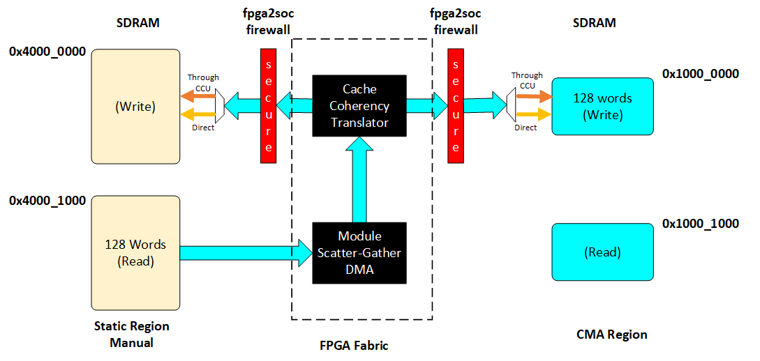
The demonstration script runs 4 tests on via a simple bash script. All the tests are run using a DMA controller in the FPGA fabric, controlled from the HPS.
- 2 sets of Read and Write Buffers are created for the DMA to use. Read and Write buffers are named from the DMA controller perspective).
- One set of Buffers is created in the manually reserved memory region.
- One set of Buffers is created in the Contiguous Memory Allocator (CMA) Area.
- The Read Buffers are populated with test data from user space prior to the test running.
- The Altera Cache Coherency Translator is set prior to each test, to set the transaction routing (SDRAM Direct or via CCU) and the AXI Transaction attributes. See Test Script for full detail on AXI Attribute settings for each test.
The description of the 4 tests that the bash scripts executes are shown next. The test makes use of the devmem2 application from the user space to perform all the operations (configuration and read/write from/to buffers).
-
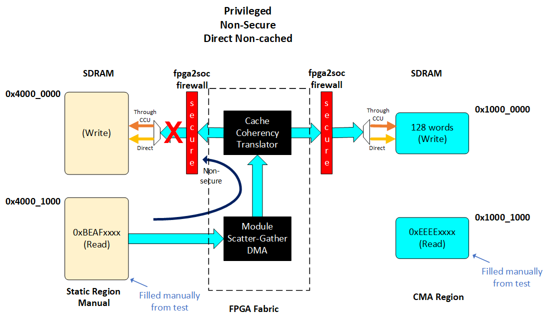
Direct to SDRAM. AXI attributes: Privileged, Non-Cached and Non-Secure access.
- Write 128 words in the read buffer at the manually reserved area of SDRAM from the user space. Read back the buffer from user space to confirm the content.
- Configure the DMA controller to move the chunk of the 128 words to the write buffer also in the manually reserved area of SDRAM.
- Read from the write buffer to verify the content. This content is should not match to the content written in the read buffer due to Non-secure transactions are being blocked by the FPGA firewall.
-
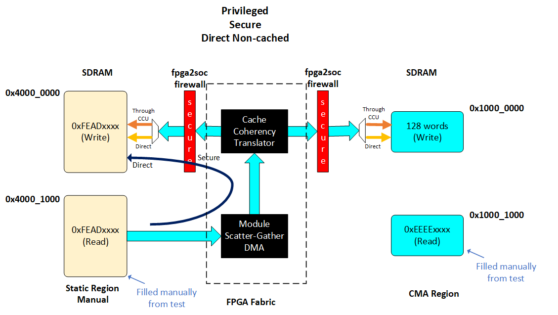
Direct to SDRAM. AXI attributes: Privileged, Non-Cached and Secure access.
- Write 128 words in the read buffer at the manually reserved area of SDRAM from the user space. Read back the buffer from user space to confirm the content.
- Configure the DMA controller to move the chunk of the 128 words to the write buffer also in the manually reserved area of SDRAM.
- Read from the write buffer to verify the content. The content in the write buffer should match with the data written in the read buffer.
-
Through CCU. AXI attributes: Privileged, Non-Cached and Secure access.
- Write 128 words in the read buffer at the manually reserved area of SDRAM from the user space. Read back the buffer from user space to confirm the content.
- Configure the DMA controller to move the chunk of the 128 words to the write buffer in the CMA reserved area of SDRAM in non-cached mode.
- Read from the write buffer to verify the content. The content in the write buffer should match with the data written in the read buffer. This test can be edited to use the manually reserved area of SDRAM as the write buffer.
-
Through CCU. AXI attributes: Privileged, Cached and Secure access.
- Write 128 words in the read buffer at the manually reserved area of SDRAM from the user space. Read back the buffer from user space to confirm the content.
- Configure the DMA controller to move the chunk of the 128 words to the write buffer in the CMA reserved area of SDRAM in cached mode.
- Read from the write buffer to verify the content. The content in the write buffer should match with the data written in the read buffer. This test can be edited to use the manually reserved area of SDRAM as the write buffer.
The following table describes the configuration that is being performed in the Cache Coherency Translator in each one of the tests and the values in each one of the fields. This configuration determines the memory transaction attributes in each test.
| Field | Test 1 Direct Non-Secured Non-Cached Privileged |
Test 2 Direct Secured Non-Cached Privileged |
Test 3 Through CCU Secured Non_cached Privileged |
Test 4 Through CCU Secured Cached Privileged |
|---|---|---|---|---|
| CSR Register | 0x7C108208 | 0x3C108208 | 0x20982302 | 0x20F82F02 |
| ARDOMAIN[1:0] | 0x0 | 0x0 | 0x2 | 0x2 |
| ARBAR[3:2] | 0x2 | 0x2 | 0x0 | 0x0 |
| ARSNOOP[7:4] | 0x0 | 0x0 | 0x0 | 0x0 |
| ARCACHE[11:8] | 0x2 | 0x2 | 0x3 | 0xF |
| AWDOMAIN[13:12] | 0x0 | 0x0 | 0x2 | 0x2 |
| AWBAR[15:14] | 0x2 | 0x2 | 0x0 | 0x0 |
| AWSNOOP[18:16] | 0x0 | 0x0 | 0x0 | 0x0 |
| AWCACHE[22:19] | 0x2 | 0x2 | 0x3 | 0xF |
| AxUSER7_1[28:23] | 0x38 AxUSER[7:0]=0xE0 |
0x38 AxUSER[7:0]=0xE0 |
0x1 AxUSER[7:0]=0x4 |
0x1 AxUSER[7:0]=0x4 |
| AxPROT[31:29] | 0x3 | 0x1 | 0x1 | 0x1 |
Note: This page was migrated from Rocketboards in 24.3.1 release. In case you need to see the content from earlier versions, please go to https://www.rocketboards.org/foswiki/Projects/SettingUpAndUsingBridgesOnAgilex and see the Revision History of that page.
Prerequisites
-
Agilex™ 7 FPGA F-Series Transceiver-SoC Development Kit (P-Tiles & E-Tile, DK-SI-AGF014EB)
- Mini USB cable for serial output.
- USB cable for on-board Altera® FPGA Download Cable II.
- SD/MMC HPS Daughtercard.
- Micro SD card.
-
Host PC with
- Linux distribution with kernel-headers/ kernel-devel and Binutils packages properly installed. Ubuntu 22.04LTS was used to create this page, other versions and distributions may work too.
- Altera® Quartus® Prime Pro Edition Version 26.1.
- Serial terminal (for example Minicom on Linux and TeraTerm or PuTTY on Windows).
Building the Example
Set up Environment
Create a top folder for this example, as the rest of the commands assume this location:
sudo rm -rf agilex7f_gsrd_bridge_example
mkdir agilex7f_gsrd_bridge_example
cd agilex7f_gsrd_bridge_example
export TOP_FOLDER=$(pwd)
Download the compiler toolchain, add it to the PATH variable, to be used by the GHRD makefile to build the HPS Debug FSBL:
cd $TOP_FOLDER
wget https://developer.arm.com/-/media/Files/downloads/gnu/14.3.rel1/binrel/\
arm-gnu-toolchain-14.3.rel1-x86_64-aarch64-none-linux-gnu.tar.xz
tar xf arm-gnu-toolchain-14.3.rel1-x86_64-aarch64-none-linux-gnu.tar.xz
rm -f arm-gnu-toolchain-14.3.rel1-x86_64-aarch64-none-linux-gnu.tar.xz
export PATH=`pwd`/arm-gnu-toolchain-14.3.rel1-x86_64-aarch64-none-linux-gnu/bin/:$PATH
export ARCH=arm64
export CROSS_COMPILE=aarch64-none-linux-gnu-
Enable Quartus tools to be called from command line:
Build Quartus Design
This Quartus project starts using the Quartus reference design for the DK-SI-AGF014EB OOBE (booting from SD Card):
cd $TOP_FOLDER
rm -rf agilex7f-ed-gsrd
wget https://github.com/altera-fpga/agilex7f-ed-gsrd/archive/refs/tags/QPDS26.1_REL_GSRD_PR.zip
unzip QPDS26.1_REL_GSRD_PR.zip
rm QPDS26.1_REL_GSRD_PR.zip
mv agilex7f-ed-gsrd-QPDS26.1_REL_GSRD_PR agilex7f-ed-gsrd
cd agilex7f-ed-gsrd
make agf014eb-si-devkit-oobe-baseline-generate-design
Update the Quartus design with the following modifications:
- Change HPS parameters related to the FPGA to HPS interface
- Changing the control interface of the Altera Cache Coherency Translator¹.
- Include the Modular Scatter-Gather DMA¹.
¹ For more information about these IPs please refer to the Embedded Peripherals IP User Guide
This can be performed automatically by using the update_ghrd_bridge_example.tcl script provided as part of this page as as an encoded data stream:
⚠️Click for instructions to retrieve update_ghrd_bridge_example.tcl from encoded data
cd agilex_soc_devkit_ghrd
base64 -d <<'EOF' | gunzip > update_ghrd_bridge_example.tcl
H4sIAFKM2mkCA61YW3OiShB+91dM7T6HReNuZR/yQAAjdRKgAI/Zp6kRRmTDLcyYaFn576cRRbwkjOb44mW+7q/7656eke9IX1B/zimKOHqL+Ay9sCW7Yn4R5RxdXb3k09twVgSYhNOJ
3O0Xvf6kR3uvEizAcoW7necB4RSvgZMiCkKK6YIkeUwl7sclbsk4Ta6mUUxvSwLMs1wqP3Q6OfGfSUhRQV/mUUFR9et3NFr7REPbRX6W5FlKU96JMxLg+isiIThc4FnOOozy3QLOSUES
ymmBX0k8p2jQc/E4CiC91fV7h5FXugN3Kq9RyjhJeUR4lKV7nkv03mojPJX4MwoBzmhBU3+JvIKkLCY8Kw5jjVJOY+yXeFzjMa/xWG7JQXFURR3q2PpXdxxD09Gq+/O91UazHhXDbBj1
Wm3GF/CML+BZ2I7lNSyu2yxUy/Qc6wEbpqc7A0UVYdEUT8FjQ/OGkEfvRqj4IqU62RRKEERpiBIWBgnBcqNxSdDshRoQ5T+226H+gLerUpQjEkMqZPNTbVc3YMlmbzNmKAnZIfFBF9Ye
PlftbuS4HtZN5e6hrP+7EHzsKLZtmPfYHdm25XhoJbdWdKiYpv5QMwkbbCp6I1T+gTGwsKbbpcXP7gUt8zlcd1XHsD3L2SP61W8z1E1IRtU1PNAVb+ToroDSsFeAR1iuCi4qlv5kW66O
oZSC5RsYT1jRNAjd3ZJct8r7qDzhqmFUa2R6IkqtTf54kHFf/v1LBO16m9HVCrY0ESFNax1AJbwrYGAr6j+6J14p29EHugdz18Fn9l/D8hK2Ui1HV7T9mvTO8NCwPiMA695RHh9LOD5z
2kC72ZYJjSrYpVUviMfmOYrpDiAx748NeCWOwpQGSPF9yhhlbeYjiOzExmilHTuGp+M6uY/DLbK/1F+/57TgSzQssxs41iM2bKxC8zxY92g1JTGjQsfd7kw4eaipWZoCH/IPrjq783Bz
uq1h+5cnadab4vgNk0WEEwJ3wOJH++Eq+ezIpR8/464sS9kcpIifBb0ANPOfD30VjEOWa1cFBW1Fna3BnaYkoFwC0p2Vf326n8hSzDCg1bUbAoP4XullXiAb6AlG25TexSukZdM/tG16
Qq7qf4Z4O9UukwRISCBSLyZ/5uWtiDgVdFMm4FKO7gijCHxCXgzxDPF19Jt9xQAE17co2OzVLevRJv+0NmsPEljzIour2qIJ0Cob1pW8kOH1DmSZD37PJGswZX4ilV9Z9yOCaR7CtbMH
QJxP2oj+8hCuqFyqjLYkey5AykOqG7l6lXQwyaJ89iX1KhdSPsF+PscyPibsbsjaCv+lMMSGybHs3XrQt8oMxDuVhbr4oypXm+JL+Tbn2TFNvz2ry4beMVXv/6LaTsYTosFlrMOWqY/L
rZpOsx3D5jlB9aADbf/LdTr5nDP0bfO0oJwXMaClb/8BgTqGBHgRAAA=
EOF
Proceed with the Quartus project build with the following instructions:
cd agilex_soc_devkit_ghrd
qsys-script --qpf=ghrd_agfb014r24b2e2v.qpf --script=update_ghrd_bridge_example.tcl --system-file=qsys_top.qsys
cd ..
make agf014eb-si-devkit-oobe-baseline-package-design
make agf014eb-si-devkit-oobe-baseline-prep
make agf014eb-si-devkit-oobe-baseline-build
The output of this stage will be:
- $TOP_FOLDER/agilex7f-ed-gsrd/agilex_soc_devkit_ghrd/output_files/ghrd_agfb014r24b2e2v.sof
You can also modify and build the Quartus project manually as indicated next. This should be done just after executing the make agf014eb-si-devkit-oobe-baseline-generate-design command in the previous instructions.
-
Open the Quartus project with the following command and then open qsys_top.qsys from Platform Designer:
-
Right-click on agilex_hps name and select Edit Parameters then configure it as follows and click on finish:
FPGA to HPS slave interface
- Interface specification → ACE-lite
- Enable/Data width → 128-bit
- Interface destination → customNote: The interface destination is set as custom because we want to control the data path to SDRAM (either direct or through CCU) from the signals in the memory transaction defined by the Cache Coherency Translator.
-
Right click to the altera_cache_coherency_translator_0 to configure the parameters as indicated next:
General
- CONTROL_INTERFACE → CSR
- Address Width → 32
- Data Width → 128
- AXM ID Width → 5
- AXM ID Width → 5
ACE-Lite Transaction Control for read Channel
- ARDOMAIN_OVERRIDE → 0x2
- ARCACHE_OVERRIDE_EN → Enable
- ARCACHE_OVERRIDE → 0xf
ACE-Lite Transaction Control for Write Channel
- AWDOMAIN_OVERRIDE → 0x2
- AWCACHE_OVERRIDE_EN → Enable
- AWCACHE_OVERRIDE → 0xf
User Selection
- AxPROT_OVERRIDE_EN → Enable
- AxPROT_OVERRIDE → 0x3
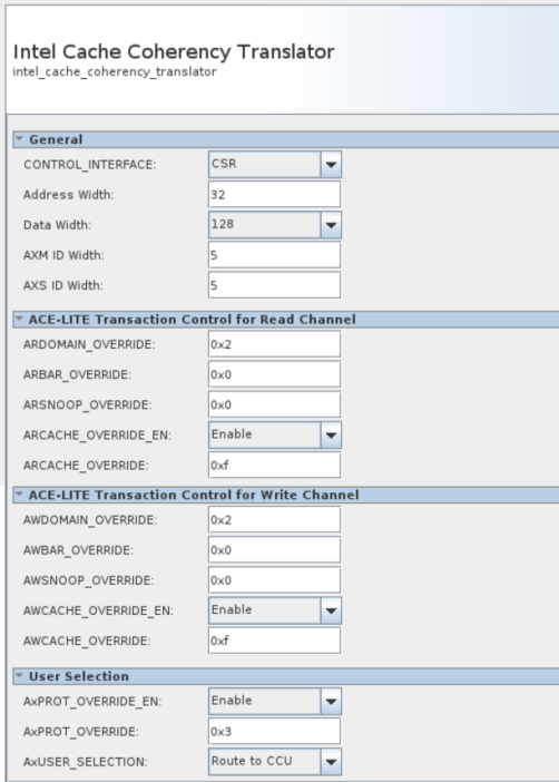
- CONTROL_INTERFACE → CSR
-
Add Modular Scatter-Gather DMA IP to the design with the following configurations:
DMA Settings
- Data Width → 128
- Data Path FIFO Depth → 512
- Descriptor FIFO Depth → 64
- Response Port → Memory-Mapped
- Maximum Transfer Length → 4KB
- Burst Enable
- Maximum Burst Count → 64
Extended Feature Options
- Enable Extended Feature Support
- Programmable Burst Enable
Pre-Fetching Options
-
Data Width of Descriptor read/write master data path → 128
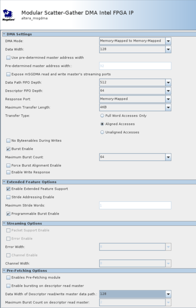
- Data Width → 128
-
Move the msgdma_0 component (Modular Scatter-Gather DMA) below the agilex_hps component selecting the component and using the UP button.

-
Connect the altera_cache_coherency_translator_0 component as shown next:
- csr_clock → clk_100.out_clk
- csr_reset → rst_in.out_reset
- csr → agilex_hps.h2f_lw_axi_master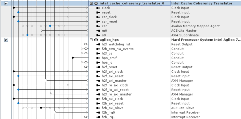
-
Connect the msgdma_0 component (Modular Scatter-Gather DMA) as shown next:
- Clock → clk_100.out_clk
- reset → rst_in.out_reset
- csr → agilex_hps.h2f_lw_axi_master
- descriptor_slave → agilex_hps.h2f_lw_axi_master
- response → agilex_hps.h2f_lw_axi_master
- mm_read → intel_cache_coherency_translator_0.s0
- mm_write → intel_cache_coherency_translator_0.s0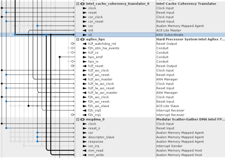
-
Use the padlock
 on the "Base" column to lock all the base addresses except the ones in Altera Cache Coherency translator and Modular Scatter-Gather DMA components. After that go to System → Assign Base Addresses menu and click it. Once the process is finished, the Address Map tab should look similar to this:
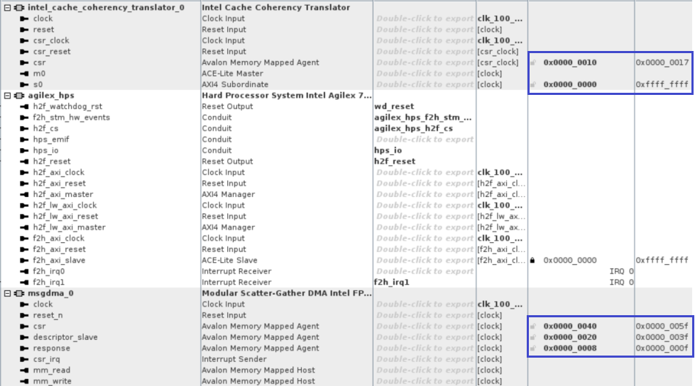
-
If everything is ok, there shouldn't be any error on the system Messages tray and you can save the design and click on Generate HDL button now.
-
Finally close Platform Designer and start building the updated Quartus design on Quartus Pro by either clicking
 or pressing CTL-L.
Rebuild the hps_debug.sof from Updated .sof
cd $TOP_FOLDER/agilex7f-ed-gsrd
# Generate hps_debug.ihex
make agf014eb-si-devkit-oobe-baseline-sw-build
quartus_pfg -c ./agilex_soc_devkit_ghrd/output_files/ghrd_agfb014r24b2e2v.sof ghrd_agfb014r24b2e2v_hps_debug.sof -o hps_path=./agilex_soc_devkit_ghrd/software/hps_debug/hps_debug.ihex
mv ghrd_agfb014r24b2e2v_hps_debug.sof agilex_soc_devkit_ghrd/output_files/
cd $TOP_FOLDER
The following files are created:
- $TOP_FOLDER/agilex7f-ed-gsrd/agilex_soc_devkit_ghrd/software/hps_debug/hps_debug.ihex - HPS Debug FSBL
- $TOP_FOLDER/agilex7f-ed-gsrd/agilex_soc_devkit_ghrd/output_files/ghrd_agfb014r24b2e2v_hps_debug.sof - FPGA configuration file, with HPS Debug FSBL
Build Core RBF
Create the Core RBF file to be used in the rootfs created by Yocto by using the HPS Debug SOF built by the Quartus design makefile:
cd $TOP_FOLDER
rm -f *jic* *rbf*
quartus_pfg -c agilex7f-ed-gsrd/agilex_soc_devkit_ghrd/output_files/ghrd_agfb014r24b2e2v_hps_debug.sof \
 ghrd_agfb014r24b2e2v.jic \
 -o device=MT25QU02G \
 -o flash_loader=AGFB014R24B2E2V \
 -o mode=ASX4 \
 -o hps=1
rm ghrd_agfb014r24b2e2v.hps.jic
The following files will be created:
- $TOP_FOLDER/ghrd_agfb014r24b2e2v.core.rbf - HPS First configuration bitstream, phase 2: FPGA fabric
Set Up Yocto
1. Make sure you have Yocto system requirements met: https://docs.yoctoproject.org/scarthgap/ref-manual/system-requirements.html#supported-linux-distributions.
The command to install the required packages on Ubuntu 22.04 is:
sudo apt-get update
sudo apt-get upgrade
sudo apt-get install openssh-server mc libgmp3-dev libmpc-dev gawk wget git diffstat unzip texinfo gcc \
build-essential chrpath socat cpio python3 python3-pip python3-pexpect xz-utils debianutils iputils-ping \
python3-git python3-jinja2 libegl1-mesa libsdl1.2-dev pylint xterm python3-subunit mesa-common-dev zstd \
liblz4-tool git fakeroot build-essential ncurses-dev xz-utils libssl-dev bc flex libelf-dev bison xinetd \
tftpd tftp nfs-kernel-server libncurses5 libc6-i386 libstdc++6:i386 libgcc++1:i386 lib32z1 \
device-tree-compiler curl mtd-utils u-boot-tools net-tools swig -y
On Ubuntu 22.04 you will also need to point the /bin/sh to /bin/bash, as the default is a link to /bin/dash:
Note: You can also use a Docker container to build the Yocto recipes, refer to https://rocketboards.org/foswiki/Documentation/DockerYoctoBuild for details. When using a Docker container, it does not matter what Linux distribution or packages you have installed on your host, as all dependencies are provided by the Docker container.
Clone the Yocto script and prepare the build:
cd $TOP_FOLDER
rm -rf gsrd-socfpga
git clone -b QPDS26.1_REL_GSRD_PR https://github.com/altera-opensource/gsrd-socfpga
cd gsrd-socfpga
. agilex7_dk_si_agf014eb-gsrd-build.sh
build_setup
Note: Run the following commands to set up again the yocto build environments, if you closed the current window (for example when rebooting the Linux host) and want to resume the next steps:
cd $TOP_FOLDER/gsrd-socfpga
. agilex7_dk_si_agf014eb-gsrd-build.sh
. ./poky/oe-init-build-env agilex7_dk_si_agf014eb-gsrd-rootfs
Customize Yocto
This section describes how to customize the Yocto recipes to use the core.rbf file created previously and also to support the required features needed in this example.
Adding our custom core.rbf
-
Copy the rebuilt core.rbf file to
$WORKSPACE/meta-intel-fpga-refdes/recipes-bsp/ghrd/filesusing the following names, as expected by the yocto recipes:- agilex7_dk_si_agf014eb_gsrd_ghrd.core.rbf
In our case we just copy the core.rbf file in the Yocto recipe location:
-
In the Yocto recipe
$WORKSPACE/meta-intel-fpga-refdes/recipes-bsp/ghrd/hw-ref-design.bb modify the agilex_gsrd_codefile location:to look like this:SRC_URI:agilex7_dk_si_agf014eb ?= "\ ${GHRD_REPO}/agilex7_dk_si_agf014eb_gsrd_${ARM64_GHRD_CORE_RBF};name=agilex7_dk_si_agf014eb_gsrd_core \ ${GHRD_REPO}/agilex7_dk_si_agf014eb_nand_${ARM64_GHRD_CORE_RBF};name=agilex7_dk_si_agf014eb_nand_core \ ${GHRD_REPO}/agilex7_dk_si_agf014eb_pr_${ARM64_GHRD_CORE_RBF};name=agilex7_dk_si_agf014eb_pr_core \ ${GHRD_REPO}/agilex7_dk_si_agf014eb_pr_persona0.rbf;name=agilex7_dk_si_agf014eb_pr_persona0 \ ${GHRD_REPO}/agilex7_dk_si_agf014eb_pr_persona1.rbf;name=agilex7_dk_si_agf014eb_pr_persona1 \ "using the following commands:SRC_URI:agilex7_dk_si_agf014eb ?= "\ file://agilex7_dk_si_agf014eb_gsrd_ghrd.core.rbf;sha256sum=xxxxxxxxx \ ${GHRD_REPO}/agilex7_dk_si_agf014eb_nand_${ARM64_GHRD_CORE_RBF};name=agilex7_dk_si_agf014eb_nand_core \ ${GHRD_REPO}/agilex7_dk_si_agf014eb_pr_${ARM64_GHRD_CORE_RBF};name=agilex7_dk_si_agf014eb_pr_core \ ${GHRD_REPO}/agilex7_dk_si_agf014eb_pr_persona0.rbf;name=agilex7_dk_si_agf014eb_pr_persona0 \ ${GHRD_REPO}/agilex7_dk_si_agf014eb_pr_persona1.rbf;name=agilex7_dk_si_agf014eb_pr_persona1 \ "OLD_URI="\${GHRD_REPO}\/agilex7_dk_si_agf014eb_gsrd_\${ARM64_GHRD_CORE_RBF};name=agilex7_dk_si_agf014eb_gsrd_core" CORE_SHA=$(sha256sum $CORE_RBF | cut -f1 -d" ") NEW_URI="file:\/\/agilex7_dk_si_agf014eb_gsrd_ghrd.core.rbf;sha256sum=$CORE_SHA" sed -i "s/$OLD_URI/$NEW_URI/g" $WORKSPACE/meta-intel-fpga-refdes/recipes-bsp/ghrd/hw-ref-design.bb -
In the same Yocto recipe delete the old SHA256 checksum for the file:
SRC_URI[agilex7_dk_si_agf014eb_gsrd_core.sha256sum] = "5d633ee561d5cc8c22b51211a144654fdc0be47ee14b07ac134074cbff84eb8b"by using the following command:
Updating Linux Kernel Configuration
In this example you need the following Linux kernel configuration options. Among these configurations it's included the capability of devmem2 command to access the memory regions where the read/write buffers are located. Yocto allows to add fragments and make the process easier. You can do this by executing the following commands:
# Add Configs to Linux needed to excercise this example
cd $TOP_FOLDER/gsrd-socfpga/
cat << EOF > $WORKSPACE/meta-intel-fpga-refdes/recipes-kernel/linux/linux-socfpga-lts/bridgesfragment.cfg
CONFIG_ALTERA_SYSID=y
CONFIG_ALTERA_MSGDMA=y
CONFIG_FPGA_BRIDGE=y
CONFIG_ALTERA_FREEZE_BRIDGE=y
CONFIG_FPGA_REGION=y
CONFIG_OF_FPGA_REGION=y
CONFIG_STACKDEPOT=y
CONFIG_STACK_HASH_ORDER=20
CONFIG_GDB_SCRIPTS=y
CONFIG_PAGE_EXTENSION=y
CONFIG_DEBUG_PAGEALLOC=y
CONFIG_DEBUG_PAGEALLOC_ENABLE_DEFAULT=y
CONFIG_PAGE_OWNER=y
CONFIG_PTDUMP_CORE=y
CONFIG_PTDUMP_DEBUGFS=y
CONFIG_DEBUG_MEMORY_INIT=y
CONFIG_DEBUG_PER_CPU_MAPS=y
CONFIG_STACKTRACE=y
CONFIG_DEBUG_KOBJECT=y
CONFIG_DEVMEM=y
CONFIG_STRICT_DEVMEM=n
CONFIG_EXCLUSIVE_SYSTEM_RAM=n
EOF

echo "kconf hardware bridgesfragment.cfg" >> $WORKSPACE/meta-intel-fpga-refdes/recipes-kernel/linux/linux-socfpga-lts/sgmii.scc
Add u-dma-buf driver to create CMA regions
It is also necessary to modify the device tree to include a 3rd party driver (u-dma-buf) to reseve the CMA memory regionlocation add the following changes to arch/arm64/boot/dts/intel/socfpga_agilex_socdk.dts to define how the memory will be allocated by u-dma-buf. This is done through a patch that will be created
as shown next.
## Create the fragment of the device tree to add u-dma-buf and reserve 256 MB of memory. Creating this as patch.
cd $TOP_FOLDER
rm -f dmaBufNodes.txt
cat << EOF > dmaBufNodes.txt
    reserved-memory {
        #address-cells = <2>;
        #size-cells = <2>;
        dma0_mem:dma0@0x10000000 {
        compatible= "shared-dma-pool";
        reusable;
        reg=<0x0  0x10000000 0x0 0x10000000>;
        label="dma0_mem";
        };
    };

    soc {
        clocks {
            osc1 {
            clock-frequency = <25000000>;
            };
        };

        udmabuf0: udmabuf@0x10000000 {
            compatible = "ikwzm,u-dma-buf";
            device-name = "udmabuf0";
            minor-number = <0>;
            size = <0x10000000>;
            memory-region = <&dma0_mem>;
            dma-coherent = <1>;
        };
    };
EOF

# Create a Linux repository in the $TOP_FOLDER
rm -rf linux-socfpga-for-patch
git clone -b QPDS26.1_REL_GSRD_PR https://github.com/altera-opensource/linux-socfpga linux-socfpga-for-patch
# Add the content of dmaBufNodes.txt  after 4 lines of finding memory@
awk '
    /memory@/ {found=NR}  # Store the line number where "memory@" is found
    {print}  # Print each line as it is
    found && NR == found + 4 {while ((getline line < "dmaBufNodes.txt") > 0) print line; found=0}  # Insert after 4 lines
' linux-socfpga-for-patch/arch/arm64/boot/dts/intel/socfpga_agilex_socdk.dts > temp.dts && mv temp.dts linux-socfpga-for-patch/arch/arm64/boot/dts/intel/socfpga_agilex_socdk.dts

## Create now the patch using the differences
cd $TOP_FOLDER/linux-socfpga-for-patch
git add  arch/arm64/boot/dts/intel/socfpga_agilex_socdk.dts
# Create the patch and add the Uptream status header to prevent QA errors
git diff --patch --staged > $WORKSPACE/meta-intel-fpga-refdes/recipes-kernel/linux/linux-socfpga-lts/socfpga_agilex_socdk.dts.patch
# Add the Upstream-status label to prevent issues
sed -i '1i Upstream-Status: Pending\n' $WORKSPACE/meta-intel-fpga-refdes/recipes-kernel/linux/linux-socfpga-lts/socfpga_agilex_socdk.dts.patch

# Include the Patch created in to the recipe
cd $TOP_FOLDER/gsrd-socfpga/
FILENAME=$WORKSPACE/meta-intel-fpga-refdes/recipes-kernel/linux/linux-socfpga-lts_%.bbappend
awk '/file:\/\/fit_kernel_agilex7_dk_si_agf014eb.its/ {sub(/"$/, " file://socfpga_agilex_socdk.dts.patch\"")} 1' $FILENAME > temp && mv temp $FILENAME

#Installing u-dma-buf driver
cd $TOP_FOLDER/gsrd-socfpga/
devtool create-workspace buff
devtool add https://github.com/ikwzm/udmabuf
bitbake-layers create-layer $WORKSPACE/meta-bridges
bitbake-layers add-layer $WORKSPACE/meta-bridges
devtool finish udmabuf  $WORKSPACE/meta-bridges
echo 'CORE_IMAGE_EXTRA_INSTALL+="udmabuf"' >> $WORKSPACE/agilex7_dk_si_agf014eb-gsrd-rootfs/conf/local.conf
Setting propper fpga2soc permissions in U-Boot
For this exercise it is required to allow only secure transactions through the fpga-to-hps bridge. This is done by default because U-Boot doesn't modifies the soc_noc_fw_mpfe_csr_inst_0_mpfe_scr register (0xF8020018) in the SDRAML3Interconnect firewall. U-Boot performs some firewall configuration using the settings defined in the soc_noc_fw_mpfe_csr_inst_0_mpfe_scr node in the arch/arm/dts/socfpga_agilex-u-boot.dtsi device tree. Please note that there is not any configuration defined for the offset 0x18, so it means that this register keeps the default configuration having the fpga2soc bit with a value of 0 indicating that only secure transactions are allowed).
Note: In previous releases, there was a patch at $WORKSPACE/meta-intel-fpga-refdes/recipes-bsp/u-boot/files/0001-HSD-14015655818-arm-dts-soc64-agilex-Enable-F2SDRAM-.patch that actually modifies the defualt configuration of this register, but in this release this patch is not longer used.
Configuring U-Boot script
To reserve the 1 GB memory for the buffers in the static region it is necessary to moify the Linux command line to add the mem=1G. The Linux command line is defined through the U-Boot boot script located at $WORKSPACE/meta-intel-fpga-refdes/recipes-bsp/u-boot/files/uboot.txt. In this file we require to modify the bootargs environment variable. This is done through the following command:
# Update u-boot script to reserve 1GB for the application
cd $TOP_FOLDER/gsrd-socfpga/
OLD_BOOTARGS="rootwait"
NEW_BOOTARGS="rootwait mem=1G"

sed  -i "s/$OLD_BOOTARGS/$NEW_BOOTARGS/g" $WORKSPACE/meta-intel-fpga-refdes/recipes-bsp/u-boot/files/uboot.txt
sed -i "s/$(echo -ne '\u200b')//g" $WORKSPACE/meta-intel-fpga-refdes/recipes-bsp/u-boot/files/uboot.txt
Copy the Test Application to Linux File System
To exercise this application, you need to have the dmaTest_cache_v2.0.run test script into the Linux file system. The test script is provided in this page as an encoded data stream which can be retreived as indicated next:
⚠️Click for instructions to retireve dmaTest_cache_v2.0.run from encoded data
cd $TOP_FOLDER/gsrd-socfpga/
base64 -d <<'EOF' | gunzip > dmaTest_cache_v2.0.run
H4sIAFKM2mkCA+0ca3PaSPIz+hV9QF1gA0TCzq6XlK8OY7zn2jjOGfuyW1spl5AG0K2QWD0Mvsv99+vuGT0AgYkh+7g6uULQTE9Pv6fnReVPr4aO92pohhNNqxzy0fAPev7sMXDGkwhq
vTq09Xa7iR+voetGIjCxOpj5gRk5vofAtxMnBMu3BZieDdFEQCBcMxI22L4VT4UXhWAGImlsJbgRYIpggWO6YYPaIq5HPw4gDgX4I8I0BUQ99h9E4CH08JGxi8UsEGEIrmMJD0FjzxYB
zCeONaH6R5iLQCCuWeA/ODa2i3zCC7XyW9miXG/BnecSDsKnShP4EHwsDeZOKBrcbmo+IjbPj4iwBkx92xk9NpiPBszioeuEkwbYThgFzjCOBH+3XJ+4CCAKTC+cOhF25YSIhwVF5YVy
mjvRxI8jJasXIRLlIPA8cKJIeDATwdQJQ5R7i/W0q+hTUZghSrTB3SBHiSgRE3biTGeugzBzM0CaI0cgIIsCEZsefhBH+DVilKqp+whhxD06BEJyV/JsHdYuK5qmTYQ7q9W1f2slYU18
eHEXmmPRgRdVy59OUQKeORXwwp+RYYZaqXQtv3Xwa6nZpNYNaE7kGwr2wXGxvd30PRc12ZytVYTCigPUZzOUVZYVN2PPMq2JsLE0zkrTMusFFmr/0TRSmRjGo5EI7kfOYmaiAgOPqbf8
2ItOdc207aBr4xeUYBB18e20amhoyK6An6DKYNDEF6N9Ah81209aVGs1fXH8lYSo17mYCqspopdVCYqVqufTalursNi4CqqqXLPFw1RM26p4nlbAX/4Mr7DylRe7rlarcWcvXyJG2/eE
tsrj74BBrG/nyg/Nbc7ITqv6Gy0UrrCi03JZUxaHFIxFhC/IE5TZ3FatbN24lmwqM6UyQNNHJLMwtsrQNKHcbGJZufrXch008WC6EArsqIlFqvsykmiii5arRpm8UdNKzcknafd1rUT/
oeMsMBQh8aU3+K85+7TmCAhZSjib+WUFGH4qcIwl0DABjT8tOwpCQQpmxQmY9QnyrkO4IIWyJJRW+qqufF0EgR8sMdE03mgII0LTQkh8KmQXFNQHM9PCMN4do50ttMrf2hf3bz8A6IvR
t7oOOj5cCPToi7Yskh9NWXCBj/yowZBk+hKOvzuDer4dQp8stcP/ztfbGa3X3JIpvOpfXd/8CG+ve93by+t3A9ACYdr30oX0ezSv2HTvkQkRPAj79BhRG0RuDsq4t6ZmBkLVbQJhX1Qw
hYj0Nag1RAyi9Xp391Ipp2Ucycyhi+aIxJ8Fjj1Guc58x0OXCTXHsqJ7KwxOpWSJVm0ajm1Emy89TktxcLUCZxb5gWs+iBSgnQIgNTO05KxKPyGx+aMRGnuYQ35v+V4U+C4CHhdjv2eZ
TTDRQBhjE5CUh+vPtyCSMAmmkw1QrvDGEUFsAhjGQYhBcWFtqM84MiwyFjb7MnEB4WN4eU6DvzNqAISYIbg2cM3QtH5G0+v2zl/3uhf9chrfUgHqMNdUKCwPRBTPoPvDJQzIgZ3oEaRS
4cHBrG5wA8pXXmL7k7JW+QcV9+6w026v33x7edvXKreU0JgWhxzKjWAoQJoLJRGe7ymPXoG0mOgh5SIURsQ4g88X2WImPNvxxuB7cCWmfvCIyZDrW5xtAnn5D3eD/g10iDDQKs3ST990
9I/4jh54TAA97r6EkIpmGDhjz3QJaQdb/GQQPMZXzGNsf2piqOQ3fWjoJfragevvOwCGDnBDQr72LEH9+ZgLYUoFNckLpq0+MaQb9U6S3AaCRgnkAFlBk42oT92AS8/DNCqcYOJE7gQj
5Bxj9YRfopyYWoCqEfDOjwSiRrtEco867YTcoRmAfIhcXZGLMN90jhOY0PP9WQ6GoSTfRufkowRiFaVABj7M94czuEnELZAW5DnPKVZ/6ELN0A0DU2joTQRanzlGCYYRai50AsrSxcR8
oKSVUtKk8q3jxQuYKn1GlCm3EJLEg0m1DTjPYGRXSxB1IvqoYyD/SPR8g7JQTx/IRWuoYVG/85xfYrFNWS34ouoyXneMY0lwsbpYFScd42sJtKYvVlct9RcMq0wAhyEgHnHGQzySdNrt
jvGtxLOu0pJS6YdUpShnTwg7pCkRzr1wwqRUYiqBE23tk077iHEuUDcB2hbLX9qSbpSUp8EpeSDZp9FpSxpwSoCzpIwXRcL7zL1Ny6IRGhUQhjg/CYGdNdOWqkfyvqc5n5vQV8tCBOpv
a6e67HSgcvfDd44h5h1HuZBi3rZ4wqQQMQVG1YBlw0QrLgo2u/g/7B0AUGgyAGA4hhxjm3wvZazAWRDD+VXrd+MIemKFkjVrEtLQ9Ps38t/Yxisc01Bk3cW5VL0MgjzO50Mgpw608sBy
at7Kb9yS8294heYAtIQT8OIKgTpsMq/Aj6Ml0wl5nCbiGKKZVSHm1ZCdBmwJu2SA3YWy1xrGe5ihkNxHyYBrUtpDPjw4v+lewTmOWVbU2JTfZOkMjlDI1tnjzAzD+hfPbSRxNhMHK1lO
Xy9pz0hulNclbt600hGSPIOdD5HUtwUcI4dih5ijchMZdIqjTgKGQ2gwRdVTYO2pkbbBLivnKtIGtgSknZnbGJVyzD0Rl/Iy2BZ3PpO5jSEJh3I50URUfR3yhvvUUAhQgl0jhQoIJllk
qzgmaRVbjHBmiXEkgqGPndF02dBP2jhRq8jukXhFu5JIIkApb1IcQGIJieFIQyOL1SpMNqjJC3+jTBwSwRuqMFcFCWjyhkgyulJXv7zp927hcHTymKmU81w6j4whDqKGxCJn+3ruq5z+
Izff9Iq5GfR7dzd9OLDwD8GU/jRTRwlT6d6D5E0uL9HaP40WHnsPBvBA/BLzFOPBdGPBg5gy4p/ZdJO1jIYKvtKUeXFaWnMDaHii0nnSx9CJYBrjDAWjNy2oYauL9gBG2M8cAdWqNs3A
IzHFnNkzxzhkBWLshLQG0gLnHuvup+PgfjQbm+3Qt+6tKHA7FNjn97KXjD8aQ+T89NB2KAULUnlGTmV55agqyFxL1qV2KLHkNJd+pcUdVNnX+sVJ+0Jva0u8NFWAAfgSUWBPrvSnuWqn
XEm23mXDPnw5Ren6RpZU1VOK0nPf9FVFfXvSPkoVleNIqeqLaer5bOlPs9XO2JJrWjxpSpMhtZx15duiTIOVWuxPVip5LQyTYV7IDzkjJCc/4gZhA2A5KcwsnL83UYjqPbeittY5hqWl
IZpw81wpjXfFpEEW5aHCaYsKHsWwRymsCmWUsXfkluD/TuSkRLfXvxkM4Or6vM97ndoTwn+Qi5ZJbGLxk/ST0LVR+mls21CfRIlE4tqulMjE77OpUZa+kRpZn+r/KWowdTNjNwq5+yQ7
Km9GnyQchz5fcNhN4cptf3A7IOahufQsO2EkQuS8WfhoFaOlMmOeuXnoMTXSWbLNVWnyAqNcNaOdFXYp6TK0GW6ypu2pmfhGlE4O1coaTnRDmsbdpIv2owDjKuX5ENJ2FdLfzojgtdNE
rbv3Hoc0DVTtCAUFeOR+ecr+GSStCYzNeZssE4ketfJrSUsLBrkpRY7PJSmrZszcKlVLYNZkVQYYdnIrPXRaQzzF5XHrt6FTFe9AIibG/du793BxfQNk75BsD33ujs6TY2bRkCkb7eqS
Zc0Z0e6+3MyF01OgfWT4+IaGAy+l/PR5T7mk2sMtWiEYnWU3T+e3HHMHycCYhl8o7919FixEGi1Y2ZGzi49mceVZUcI2I1MdWUi2jU/1xVm/e8Gbt+vVBlb31YPNeZPVtO/VJi5vfVa3
bUKvN5E7oel2MdXLLdIlnNv2owvarCBlg4eloV/bx3h3ztOaed0281bUyeVnhV39P38ryt804a7HgzCNB3u440ooaG8KBemM51BxgIKAGqzNosF6t0Bw6MG6ODJc9Lvn//ORYZ+x8NeY
wf0/AKwEACvOAkDpGZ644vpHHVhZ41h3/ue5fJm2Wjbnsr9dzopkOGPSh6n2Q1dAqCvSnqwk51ebDdxza0O06OKzJVror+XfbxYt8ifWUEJfJMD8OvHlMEsDO68MFDqhlcvKP881Vvzv
uJNfcDmE77Hfya1rnm0eztE+Z9aVPwkpPHUQEmBf52u1QF1XuKRbAd7PDGwGU0lb2Nrknuf4/HHc8zme9qVX9nZd2Bs5B172+kLrX/nbEZWbu3dqdeDzZuxLk3fZ9NJzIkeeMceYR0fg
Wxiq5hDEnkdpa6QcE225rGm/xrJCAZE9tFc+ATLzZ7G69pL3Ndqd3mr0FA9ijw8gJtvd5tB/EGB8d1YHYqzghsOTSKsFzpuISJ5ylFQ+8hFeot/AGGrKw+v5E7zbu9lLgDtLECXUu+pm
U5gkeibHBlfIXD6dnsVFDovlXeS5gqFAmMbewlzpYz9JViwrVqOEWvnKhg3AYTYZOFZmvD1XmAHRK/WqxgoleCR3WxKz3W4xUOJY0JV/5U03kZ7sg+/gJGjq9ecJfWsPe8k9dIWYwWtt
VZyo2e2yXFL9dvOWkjyTf7tLcqkHJUeF5CByXDHeg0iRBrxnI0oC8oXjOZybjRyXT6RJguW1RvnhqIGFGC/v36PMyc9Rher6hEvXFX3ge2JyqoYEECmyw9ylCkkb6qZalC3VofkXeax8
BXAtB6rTOFEBNWI6/1LrQUzAOmFMEt1XJXowA4r8GQ+mtoMhMpIHDf9Jk3LH48tcThQmg26rVW/IbJ2UjxBRC3NknHbQ1SM+H3asKwblDRM690X4U9xBbiCu1arZdZqX1fWrNfU6cHJk
FONML6+Ez0HaXqP0hnk6z0iF56AlVfQXkTzRn9Go8hiaU9CIJ/JVGAKUu2vrNKGdKHdsAKCyUXFH7SEqpQHxbJa+cRZaLUyhC60rJ7LCy0DMTGHLIqEst31ZfeI+FAprvpHcVRFIF0hl
sIsI1nP+YscpP5+X9NpWovjiHvbtYFVac1ra3SoueQuMbGr4SEu2x/rXJ2g5RvuEVtsWKKs9uJbIFUFtfc2FzuiGGfDN1RB7aqDV/xILuk/gxdMhauoUjD265wts3Dt331YHft5AhV7o
TI+BcZBuweO0DLuC2twPUv+h4zUY0wJBt9IB1fbuVRdDCQPTJfY4oPO67iMkVw5pPZIi4+V7nBbC6r22I53ooNBnIBFv0iucRvaNLmJX5DBLV9TjcFVesm7AdeseqY4L0QElwiMDTYdi
yHd+qVRCXm+SMbhUkjPaygcTtUyniqTbIMCMAPtmQIzhLAohtcrtAvpBAPxxefN31ZoRSMhbEUxVDUP3/OnMFYgQy4DKkp4ZoO+xrPrX7/n1vRn8LPsPs3fyc/mKYMj6uRQycNEgX1QC
7oHPt4M1MT06E5wRqE4iG7lLs2tilaJCs58n4qB7nXtYXhbl2fak6WHvaHr6Rnr2mFj+gZqiJdIRxd1UwJnJ2M80sZ8q9MWJ0sQbpKHQNCqlyxH/8gUSEgKOsgLjExnzIt2p0OES5skF
CrkpRrFT7W/IvQ4Oxw3+DQ4TCARNVwYXBuJjm/s6+t76u1E5PC8mcmLP09/8ZISuVMJTByQA1NoqqB2hD1QsFsKKea5O66tCrq9e0+GD3B41Lck0ZN/y4rC8Kkxyk9f9uEr9mkiLVmW3
b84mpPzox+vXjk1IJkCc2VOsHtF+Fa0J0LbjAp/yk7s/z+yAdio2d2Dt3wGttcoOaGqUafgsXSr+7HRny89ibMxgCn4s4xg+orPt84sZKz+CUfBzFxtW6xNTJzPmlcbz63d92La+X9ay
NVkkUM/upGsV7v1Uq/AvJZyqao4iWqWW/oACFgP9mke+5GStxOIShSmr0CorvTP6OcU9pXpi+s3OYAeE0v4Lizl4I8RJAAA=
EOF
Then you need to include this script into the Linux file system with the following instructions:
cd $TOP_FOLDER/gsrd-socfpga/
mv dmaTest_cache_v2.0.run meta-intel-fpga-refdes/recipes-gsrd/socfpga-gsrd-apps/files/
# Adding this to the list of files to be copied to the file system
sed -i '/file:\/\/README_agilex5/a\\t\tfile:\/\/dmaTest_cache_v2.0.run\\'  meta-intel-fpga-refdes/recipes-gsrd/socfpga-gsrd-apps/socfpga-gsrd-apps_1.0.bb
sed -i '/alteraFPGA\/syschk/a\\tinstall -m 0755 \${WORKDIR}\/dmaTest_cache_v2.0.run \${D}\/home\/root\/'  meta-intel-fpga-refdes/recipes-gsrd/socfpga-gsrd-apps/socfpga-gsrd-apps_1.0.bb
sed -i '/FILES:\${PN} =/a\\t\t   \/home\/root\/dmaTest_cache_v2.0.run \\' meta-intel-fpga-refdes/recipes-gsrd/socfpga-gsrd-apps/socfpga-gsrd-apps_1.0.bb
# Remove QA check for the new file INSANE_SKIP
sed -i '/INSANE_SKIP:\${PN} =/aINSANE_SKIP:\${PN} \+= " file-rdeps"'  meta-intel-fpga-refdes/recipes-gsrd/socfpga-gsrd-apps/socfpga-gsrd-apps_1.0.bb
sed -i '/INSANE_SKIP:\${PN}-dev =/aINSANE_SKIP:\${PN} \+= " file-rdeps"'  meta-intel-fpga-refdes/recipes-gsrd/socfpga-gsrd-apps/socfpga-gsrd-apps_1.0.bb
Build Yocto
Now that we are setup we have to execute the following command to start building:
Once the build is completed successfully, you will see the following two folders are created:
- agilex7_dk_si_agf014eb-gsrd-rootfs: area used by OpenEmbedded build system for builds. Description of build directory structure https://docs.yoctoproject.org/ref-manual/structure.html#the-build-directory-build
- agilex7_dk_si_agf014eb-gsrd-images: the build script copies here relevant files built by Yocto from the agilex7_dk_si_agf014ea-gsrd-rootfs/tmp/deploy/images/agilex7_dk_si_agf014ea folder, but also other relevant files.
For this example, the two most relevant files created in the $TOP_FOLDER/gsrd_socfpga/agilex7_dk_si_agf014ea-gsrd-images folder are:
- u-boot-agilex-socdk-gsrd-atf/u-boot-spl-dtb.hex: U-Boot SPL Hex file
- gsrd-console-image-agilex7.wic: SD Card image
Building QSPI Flash Image
The QSPI image will contain the SDM firmware, the 1st phase of FPGA configuration data and the HPS FSBL. This is built using the following command:
cd $TOP_FOLDER
rm -f *jic* *rbf*
quartus_pfg -c agilex7f-ed-gsrd/agilex_soc_devkit_ghrd/output_files/ghrd_agfb014r24b2e2v.sof \
ghrd_agfb014r24b2e2v.jic \
-o hps_path=gsrd-socfpga/agilex7_dk_si_agf014eb-gsrd-images/u-boot-agilex7-socdk-gsrd-atf/u-boot-spl-dtb.hex \
-o device=MT25QU02G \
-o flash_loader=AGFB014R24B2E2V \
-o mode=ASX4 \
-o hps=1
The following file will be created:
- $TOP_FOLDER/ghrd_agfb014r24b2e2v.hps.jic - Flash image for HPS First configuration bitstream, phase 1: HPS and DDR
Running the Example
In order to excercise this example you will need to program the binaries that you built in the previous seccion:
- SD Card:
$TOP_FOLDER/gsrd_socfpga/agilex7_dk_si_agf014ea-gsrd-images/gsrd-console-image-agilex7.wic - QSPI:
$TOP_FOLDER/ghrd_agfb014r24b2e2v.hps.jic
When using the above SD Card image, this already includes the dmaTest_cache_v2.0.run application that is used to exercise this example. This is a bash script is located at the /home/root/ directoy in Linux which is running in the development kit.
Note: Make sure that the variables in the script used to define the addresses for the configuration registers for the Cache Coherency Translator and Modular Scatter-Gather DMA components match the ones set in the Quartus design.
The addresses set in the Quartus design are defined at the lwsoc2fpga bridge with a base address of 0xF9000000:
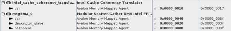
These variables are defined in the script as:
#Bridges pointers
icct_csr=0xf9000010
msgdma_csr=0xf9000040
msgdma_descriptorslave=0xf9000020
msgda_response=0xf9000008
To execute the sample test script:
- Power cycle the board to boot to Linux.
- Identify the dmaTest_cache_v2.0.run test script in your
/home/rootdirectory. -
You can see how to exercise the script by using the -h switch:
From this menu, each one of the options executes each one of the 4 tests described earlier in the Testing of the Project section.root@agilex:~# bash dmaTest_cache_v2.0.run -h Usage: dmaTest_cache_v2.0.run options Options: --help, -h --privilaged-only, -p --privilaged-secure, -s --ccu-uncached, -u --ccu-cached, -cOption Test Description -p Test 1 Direct to SDRAM. AXI attributes: Privileged, Non-Cached and Non-Secure access. -s Test 2 Direct to SDRAM. AXI attributes: Privileged, Non-Cached and Secure access. -u Test 3 Through CCU. AXI attributes: Privileged, Non-Cached and Secure access. -c Test 4 Through CCU. AXI attributes: Privileged, Cached and Secure access.
The following capture is an example of executing the Test 3.
In this test you can see that the read buffer is being written with a 0xAAAAxxxx pattern of 128 words (512 bytes). Then the Cache Coherency Translator is configured to send Privileged Secure Non-cached transactions (with a value of 0x20982302 in the CSR register) and the Modular Scatter-Gather DMA is being configured transfer a block of 512 bytes from the read buffer in the manual region (at address 0x41000000) to the CMA region (at address 0x10000000). You can confirm from the log that the data read from the write buffer also contains the 0xAAAAxxxx pattern indicating that the data was correctly transferred.
root@agilex7dksiagf014eb:~# ./dmaTest_cache_v2.0.run -u
read sysID perif,  should read back 0xACD5CAFE
/dev/mem opened.
Memory mapped at address 0xffff8e5c5000.
Read at address  0xF9000000 (0xffff8e5c5000): 0xACD5CAFE
Setup AXI Security Bridge via CSR H2F_LW + 0x8
Read ACE-LITE Bridge Mode
/dev/mem opened.
Memory mapped at address 0xffff88d1c000.
Read at address  0xF9000010 (0xffff88d1c010): 0x60F82F02
########################################
============================================
 Test 3: CCU Non-cached Privileged Secure
============================================
Setup AXI Security Bridge via CSR H2F_LW + 0x8
Set ACE-LITE Bridge to via CCU Non-Cached Mode : 0x60F82F02
/dev/mem opened.
Memory mapped at address 0xffff8bdb8000.
Read at address  0xF9000010 (0xffff8bdb8010): 0x60F82F02
Write at address 0xF9000010 (0xffff8bdb8010): 0x20982302, readback 0x20982302
###################################################
Initial setup done. Now running the test...
Read ACE-LITE Bridge Mode
/dev/mem opened.
Memory mapped at address 0xffff922b8000.
Read at address  0xF9000010 (0xffff922b8010): 0x20982302
###################################################
Creating populated data buffer at 0x40001000 in unused memory (above 1GB)
Check data by reading 1st address
/dev/mem opened.
Memory mapped at address 0xffff89529000.
Read at address  0x40001000 (0xffff89529000): 0xAAAA0000
###################################################
Creating populated data buffer at in CMA reserved cached memory at 0x10002000 from userspace
Check data by reading 1st address
/dev/mem opened.
Memory mapped at address 0xffffbe775000.
Read at address  0x10002000 (0xffffbe775000): 0x05050505
###################################################
##################################################
Finished filling buffers with with initial data
##################################################
Setup DMA controller to start transfering data
read buffer(0x40001000) -> Write buffer(0x10000000)
msgdma : Stop dispatcher
/dev/mem opened.
Memory mapped at address 0xffffbcd0b000.
Read at address  0xF9000044 (0xffffbcd0b044): 0x00000000
Write at address 0xF9000044 (0xffffbcd0b044): 0x00000001, readback 0x00000001
msgdma : Stop descriptors
/dev/mem opened.
Memory mapped at address 0xffff9fd64000.
Read at address  0xF9000044 (0xffff9fd64044): 0x00000001
Write at address 0xF9000044 (0xffff9fd64044): 0x00000020, readback 0x00000020
msgdma : Reset Dispatcher
/dev/mem opened.
Memory mapped at address 0xffffb7832000.
Read at address  0xF9000044 (0xffffb7832044): 0x00000020
Write at address 0xF9000044 (0xffffb7832044): 0x00000002, readback 0x00000002
msgdma : Read address,  lower 32bits, upper 32bits : 0x0000000040001000
/dev/mem opened.
Memory mapped at address 0xffff927d3000.
Read at address  0xF9000020 (0xffff927d3020): 0x00000000
Write at address 0xF9000020 (0xffff927d3020): 0x40001000, readback 0x40001000
/dev/mem opened.
Memory mapped at address 0xffffbe12b000.
Read at address  0xF9000034 (0xffffbe12b034): 0x00000000
Write at address 0xF9000034 (0xffffbe12b034): 0x00000000, readback 0x00000000
msgdma : Write address, lower 32bits, upper 32bits : 0x0000000010000000
/dev/mem opened.
Memory mapped at address 0xffff9ebe8000.
Read at address  0xF9000024 (0xffff9ebe8024): 0x00000000
Write at address 0xF9000024 (0xffff9ebe8024): 0x10000000, readback 0x10000000
/dev/mem opened.
Memory mapped at address 0xffff8342c000.
Read at address  0xF9000038 (0xffff8342c038): 0x00000000
Write at address 0xF9000038 (0xffff8342c038): 0x00000000, readback 0x00000000
msgdma : length in bytes 4068,  128bit x 32
/dev/mem opened.
Memory mapped at address 0xffff840ef000.
Read at address  0xF9000028 (0xffff840ef028): 0x00000000
Write at address 0xF9000028 (0xffff840ef028): 0x00000200, readback 0x00000200
msgdma : Burst counts 32, sequence number = 1
/dev/mem opened.
Memory mapped at address 0xffff99381000.
Read at address  0xF900002C (0xffff9938102c): 0x00000000
Write at address 0xF900002C (0xffff9938102c): 0x20200001, readback 0x20200001
msgdma : Check Status
/dev/mem opened.
Memory mapped at address 0xffffa2ada000.
Read at address  0xF9000040 (0xffffa2ada040): 0x0000000A
msgdma : Control,  wait for resp
/dev/mem opened.
Memory mapped at address 0xffffbeb74000.
Read at address  0xF900003C (0xffffbeb7403c): 0x00000000
Write at address 0xF900003C (0xffffbeb7403c): 0x02000000, readback 0x02000000
###################################################
###################################################
###################################################
###################################################
msgdma : Control,  wait for resp and go
/dev/mem opened.
Memory mapped at address 0xffffb94d4000.
Read at address  0xF900003C (0xffffb94d403c): 0x00000000
Write at address 0xF900003C (0xffffb94d403c): 0x82000000, readback 0x82000000
msgdma : Check Status
/dev/mem opened.
Memory mapped at address 0xffffbea2d000.
Read at address  0xF9000040 (0xffffbea2d040): 0x00000002
###################################################
Reading back data from write buffer.
ReadBack from 0x0000000010000000
/dev/mem opened.
Memory mapped at address 0xffff98323000.
Read at address  0x10000000 (0xffff98323000): 0xAAAA0000
/dev/mem opened.
Memory mapped at address 0xffff95cb4000.
Read at address  0x10000004 (0xffff95cb4004): 0xAAAA0004
/dev/mem opened.
Memory mapped at address 0xffffae5f8000.
Read at address  0x10000008 (0xffffae5f8008): 0xAAAA0008
/dev/mem opened.
Memory mapped at address 0xffffab644000.
Read at address  0x1000000C (0xffffab64400c): 0xAAAA000C
/dev/mem opened.
Memory mapped at address 0xffff8b494000.
Read at address  0x10000010 (0xffff8b494010): 0xAAAA0010
=================
    TEST DONE
=================
Notices & Disclaimers
Altera® Corporation technologies may require enabled hardware, software or service activation. No product or component can be absolutely secure. Performance varies by use, configuration and other factors. Your costs and results may vary. You may not use or facilitate the use of this document in connection with any infringement or other legal analysis concerning Altera or Intel products described herein. You agree to grant Altera Corporation a non-exclusive, royalty-free license to any patent claim thereafter drafted which includes subject matter disclosed herein. No license (express or implied, by estoppel or otherwise) to any intellectual property rights is granted by this document, with the sole exception that you may publish an unmodified copy. You may create software implementations based on this document and in compliance with the foregoing that are intended to execute on the Altera or Intel product(s) referenced in this document. No rights are granted to create modifications or derivatives of this document. The products described may contain design defects or errors known as errata which may cause the product to deviate from published specifications. Current characterized errata are available on request. Altera disclaims all express and implied warranties, including without limitation, the implied warranties of merchantability, fitness for a particular purpose, and non-infringement, as well as any warranty arising from course of performance, course of dealing, or usage in trade. You are responsible for safety of the overall system, including compliance with applicable safety-related requirements or standards. © Altera Corporation. Altera, the Altera logo, and other Altera marks are trademarks of Altera Corporation. Other names and brands may be claimed as the property of others.
OpenCL* and the OpenCL* logo are trademarks of Apple Inc. used by permission of the Khronos Group™.
Created: March 26, 2025