1.0 FPGA AI Suite PCIe-based System Example Design
The FPGA AI Suite Design Example User Guides describe the design and implementation for accelerating AI inference using the FPGA AI Suite, Intel® Distribution of OpenVINO™ toolkit, and various development boards (depending on the design example). They share a common introduction between each document, which serves as an introduction to the material. Section 4.0 begins the ED specific material.
About the FPGA AI Suite Documentation Library
Documentation for the FPGA AI Suite is split across a few publications. Use the following table to find the publication that contains the FPGA AI Suite information that you are looking for:
Table 1. FPGA AI Suite Documentation Library
| Title and Description | Link |
|---|---|
| Release Notes Provides late-breaking information about the FPGA AI Suite including new features, important bug fixes, and known issues. |
Link |
| FPGA AI Suite Handbook Get up and running with the FPGA AI Suite by learning how to initialize your compiler environment and reviewing the various design examples and tutorials provided with the FPGA AI Suite Describes the use modes of the graph compiler ( dla_compiler). It also provides details about the compiler command options and the format of compilation inputs and outputs. |
Link |
2.0 FPGA AI Suite Design Examples
The following is a comprehensive list of the available FPGA AI Suite Design Example User Guides.
Table 2. FPGA AI Suite Design Examples Descriptions
| Design Example | Description |
|---|---|
| PCIe-attach design example | Demonstrates how OpenVINO toolkit and the FPGA AI Suite support the look-aside deep learning acceleration model. This design example targets the Terasic* DE10-Agilex™ Development Board (DE10-Agilex-B2E2). |
| OFS PCIe-attach design example | Demonstrates the OpenVINO toolkit and the FPGA AI Suite that target Open FPGA Stack (OFS)-based boards. This design example targets the following Open FPGA Stack (OFS)-based boards: * Agilex™ 7 FPGA I-Series Development Kit ES2 (DK-DEV-AGI027RBES) * Silicom FPGA SmartNIC N6001-PL Platform (without Ethernet controller) |
| Hostless DDR-Free design examples | Demonstrates hostless DDR-free operation of the FPGA AI Suite IP. Graph filters, bias, and FPGA AI Suite IP configurations are stored in internal memory on the FPGA device. This design example targets the Agilex™ 7 FPGA I-Series Development Kit ES2 (DK-DEV-AGI027RBES). |
| Hostless JTAG design example | Demonstrates the step-by-step sequence of configuring FPGA AI Suite IP and starting inference by writing into CSRs directly via JTAG. This design example targets the Agilex™ 5 FPGA E-Series 065B Modular Development Kit (MK-A5E065BB32AES1). |
| SoC design example | Demonstrates how OpenVINO toolkit and the FPGA AI Suite support the CPU-offload deep-learning acceleration model in an embedded system. The design example targets the following development boards: * Agilex™ 3 FPGA and SoC C-Series Development Kit (DK-A3W135BM16AEA) * Agilex™ 5 FPGA E-Series 065B Modular Development Kit (MK-A5E065BB32AES1) * Agilex™ 7 FPGA I-Series Transceiver-SoC Development Kit (DK-SIAGI027FC) * Arria® 10 SX SoC FPGA Development Kit (DK-SOC-10AS066S) |
Table 3. FPGA AI Suite Design Examples Properties Overview
| Example | Design Type | Target FPGA Device | Host | Memory | Stream* | Design Example Identifier** | Supported Development Kit |
|---|---|---|---|---|---|---|---|
| PCIe-Attached | Agilex™ 7 | External host processor | DDR | M2M | agx7_de10_pcie | Terasic DE10-Agilex™ Development Board (DE10-Agilex™-B2E2) | |
| PCIe-Attached | Agilex™ 7 | External host processor | DDR | M2M | agx7_iseries_ofs_pcie | Agilex™ 7 FPGA I-Series Development Kit ES2 (DK-DEV-AGI027RBES) | |
| PCIe-Attached | Agilex™ 7 | External host processor | DDR | M2M | agx7_n6001_ofs_pcie | Silicom FPGA SmartNIC N6001-PL Platform (without Ethernet controller) | |
| Hostless DDR-Free | Agilex™ 7 | Hostless | DDR-Free | Direct | agx7_iseries_ddrfree | Agilex™ 7 FPGA I-Series Development Kit ES2 (DK-DEV-AGI027RBES) | |
| Hostless JTAG Attached | Agilex™ 5 | Hostless | DDR | M2M | agx5e_modular_jtag | Agilex™ 5 FPGA E-Series 065B Modular Development Kit (MK-A5E065BB32AES1) | |
| SoC | Agilex™ 3 | On-device HPS | DDR | M2M | agx3_soc_m2m |
Agilex™ 3 FPGA and SoC C-Series Development Kit (DK-A3W135BM16AEA) | |
| SoC | Agilex™ 5 | On-device HPS | DDR | M2M and S2M | agx5_soc_m2m agx5_soc_s2m |
Agilex™ 5 FPGA E-Series 065B Modular Development Kit (MK-A5E065BB32AES1) | |
| SoC | Agilex™ 7 | On-device HPS | DDR | M2M and S2M | agx7_soc_m2m agx7_soc_s2m |
Agilex™ 7 FPGA I-Series Transceiver-SoC Development Kit (DK-SIAGI027FC) | |
| SoC | Arria® 10 | On-device HPS | DDR | M2M and S2M | a10_soc_m2m a10_soc_s2m |
Arria® 10 SX SoC FPGA Development Kit (DK-SOC-10AS066S) |
*For the Design Example Identifier column, these entries are the value to use with the FPGA AI Suite Design Example Utility (dla_build_example_design.py) command to build the design example
**For the Stream column, the entries are defined as follows:
M2M FPGA AI Suite runtime software running on the external host transfers the image (or data) to the FPGA DDR memory.
S2M Streaming input data is copied to FPGA on-device memory. The FPGA AI Suite runtime runs on the FPGA device (HPS or RTL state machine). The runtime is used only to coordinate the data transfer from FPGA DDR memory into the FPGA AI Suite IP.
Direct Data is streamed directly in and out of the FPGA on-chip memory.
3.0 Shared Design Example Components
3.1. FPGA AI Suite Design Example Utility
The main entry point into the example design build system is the FPGA AI Suite design example utility (dla_build_example_design.py). This utility coordinates different aspects of building a design example, from the initial project configuration to extracting area metrics after a compile completes. With this utility, you can create bitstreams from custom AI Suite IP architecture files and with a configurable number of instances.
Note: There is no '.py' extension on dla_build_example_design when using the FPGA AI Suite on Windows.
To use the FPGA AI Suite design example build utility, ensure that your local development environment has been setup according to the steps in "Installing FPGA AI Suite Compile and IP Generation Tools" in FPGA AI Suite Handbook.
3.1.1. The dla_build_example_design.py Command
The FPGA AI Suite design example utility (dla_build_example_design.py) configures and compiles the bitstreams for the FPGA AI Suite design examples. The command has the following basic syntax:
where [action] is one of the following actions:
Table 4. Design Example Utility Actions
| Action | Description |
|---|---|
list |
List the available example designs. |
build |
Build an example design. |
qor |
Generate QoR reports. |
quartus-compile |
Run a Quartus® Prime compile. |
scripts |
Managed the build support scripts. |
Some of the command actions have different additional required and optional parameters. Use the command help to see a list of available options for the command and its actions.
By default, the dla_build_example_design.py command always instructs the dla_create_ip command to create licensed IP. If no license can be found, inference-limited, unlicensed RTL is generated. The build log indicates if the IP is licensed or unlicensed. For more information about licensed and unlicensed IP, refer to "The --unlicensed/--licensed Options" in FPGA AI Suite IP Reference Manual.
Getting dla_build_example_design.py Command Help
For general help with the command and to see the list of available actions, run the following command:
For help with a command actions and to the list of available options and arguments required for an action, run the following command:
Command Logging and Debugging
By default, the FPGA AI Suite design example utility logs its output to a set location in the (default) build_platform directory. Override this location by specifying the --logfile logfile option.
For extra debugging output, specify the --debug option.
Both the logging and debugging options must be specified before the command action.
3.1.2. Listing Available FPGA AI Suite Design Examples
To list the available FPGA AI Suite design examples, run the following command:
This command shows the design example identifiers (used with the build action of the design example utility) along with a short description of the design example and its target Quartus Prime version.
A list of the design examples and their identifiers is also available in FPGA AI Suite Design Examples Properties Overview.
3.1.3. Building FPGA AI Suite Design Examples
To build FPGA AI Suite design examples, specify the build option of the design example utility.
In the most simple case of building a design example for an existing architecture, you can build a design example with the following command:
For example, use the following command to build the Agilex™ 7 PCIe-based design example that targets the DE10-Agilex-B2E2 board using the AGX7_Generic architecture:
dla_build_example_design.py build \
agx7_de10_pcie \
$COREDLA_ROOT/example_architectures/AGX7_Generic.arch
The default build directory is build_platform. The utility creates the folder if it does not exist. To specify a different build directory, specify the --output-dir <directory> option:
dla_build_example_design.py build \
--output-dir <directory> \
<design_example_identifier> \
<architecture file>
Be default, the utility also prevents the build directory from being overwritten. You can override this behavior with the --force option.
After the build is complete, the build directory has the following files and folders:
- coredla_ip/ This folder contains the RTL for the configured FPGA AI Suite IP.
- hw/
This folder contains the Quartus Prime or Open FPGA Stack (OFS) project files. It also includes its own self-contained copy of the contents of the
coredla_ip/folder
- .build.json This contents of this file (sometimes referred to as the "build context" file) allow the build to be split into multiple steps.
- Reports
The build directory will contain any log files generated by the build utility (such as
build.log) and the QoR summary that is generated by a successful compilation.
- Bitstreams
This build directory will contain the bitstreams to program the target FPGA device as follows:
- For OFS-based designs,
.gbsfiles. - For other designs,
.sofand.rbffiles.
- For OFS-based designs,
3.1.3.1. Staging FPGA AI Suite Design Example Builds
The FPGA AI Suite design example utility supports staged builds via the --skip-compile option. When you specify this option, the utility creates the build folder and prepares the Quartus Prime or Open FPGA Stack (OFS) project but does not run compilation.
With a staged design example build flow, you must run the utility a few times to generate the same outputs as the regular build flow. For a complete build with a staged build flow, you would run the following commands:
dla_build_example_design.py build --skip-compile \
<design_example_identifier> \
<architecture file>
dla_build_example_design.py quartus-compile build_platform
# Optional: Generate QoR summary
dla_build_example_design.py qor build_platform
Information about the build configuration, namely what was passed into the dla_build_example_design.py build command, is stored inside of the build context (.build.json) file.
You can run the dla_build_example_design.py quartus-compile and dla_build_example_design.py qor commands multiple times. An example of when running these commands multiple times can be useful is when you have to recompile the bitstream after removing an unnecessary component from the design example.
You can also directly call the design compilation script. An FPGA AI Suite design example uses one of the following scripts, depending on whether the design example can built in a WSL 2 environment:
- generate_sof.tcl Design examples with this design compilation script can be built in a WSL 2 environment.
- build_project.sh Design examples with this design compilation script cannot be built in a WSL 2 environment.
If a design example uses a generate_sof.tcl script, then you can invoke the design compilation script either after opening the design example project in Quartus Prime or by running the following command:
If a design example uses the build_project.sh build script, the script must be executed in a Bash-compatible shell. For example:
For both design example compilation scripts, the current working directory must be the hw/ directory.
3.1.3.2. WSL 2 FPGA AI Suite Design Example Builds
Staged builds allow the build utility to support hybrid Windows/Linux compilation in a WSL 2 environment on a Windows system. In a WSL 2 environment, FPGA AI Suite is installed in the WSL 2 Linux guest operating system while Quartus Prime is installed in the Windows host operating system.
Restriction: Only a subset of the FPGA AI Suite design examples can be build in a WSL 2 environment. For a list of design examples that support WSL 2, run the following command:
When you run the dla_build_example_design.py build command, the WSL 2 flow is enabled with the --wsl option. This option tells the utility to resolve the path to the build directory as a Windows file path instead of a Linux file path. The utility displays messages that provide you with more details about how to use the staged build commands to complete the compilation in your WSL 2 environment.
Important: If you specify a build directory in a WSL 2 environment with the --output-dir options, that build directory must be a relative path. This requirement is due to a limitation in how the WSL 2 environment maps paths between the Linux guest and Windows.
3.2. Example Architecture Bitstream Files
The FPGA AI Suite provides example Architecture Files and bitstreams for the design examples. The files are located in the FPGA AI Suite installation directory.
3.3. Design Example Software Components
The design examples contain a sample software stack for the runtime flow.
For a typical design example, the following components comprise the runtime stack:
- OpenVINO Toolkit (Inference Engine, Heterogeneous Plugin)
- FPGA AI Suite runtime plugin
- Vendor-provided FPGA board driver or OPAE driver (depending on the design example)
The design example contains the source files and Makefiles to build the FPGA AI Suite runtime plugin. The OpenVINO component (and OPAE components, where used) is external and must be manually preinstalled.
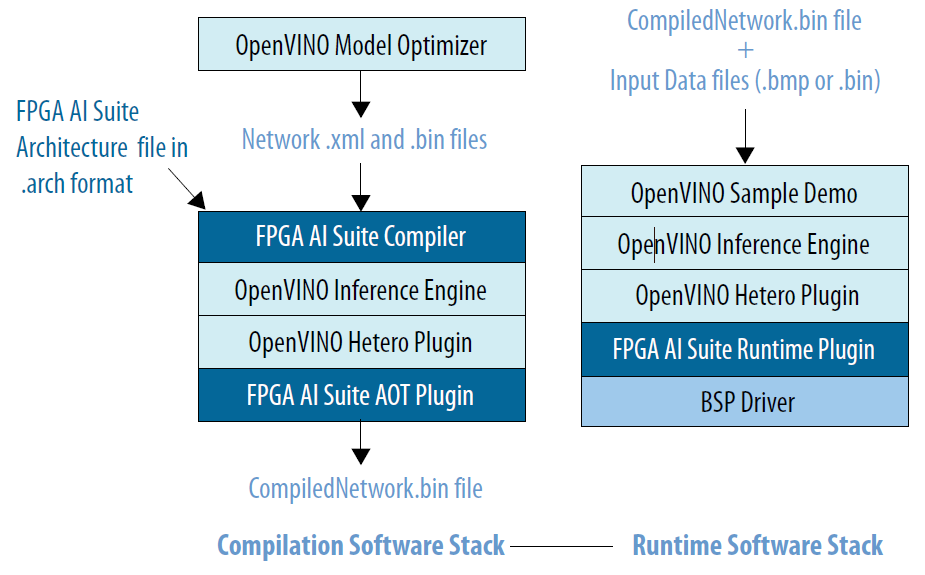
A separate flow compiles the AI network graph using the FPGA AI Suite compiler, as shown in Figure 1 Software Stacks for FPGA AI Suite Inference that follows as the Compilation Software Stack.
The compilation flow output is a single binary file called CompiledNetwork.bin that contains the compiled network partitions for FPGA and CPU devices along with the network weights. The network is compiled for a specific FPGA AI Suite architecture and batch size. This binary is created on-disk only when using the Ahead-Of-Time flow; when the JIT flow is used, the compiled object stays in-memory only.
An Architecture File describes the FPGA AI Suite IP architecture to the compiler. You must specify the same Architecture File to the FPGA AI Suite compiler and to the FPGA AI Suite design example utility (dla_build_example_design.py).
The runtime flow accepts the CompiledNetwork.bin file as the input network along with the image data files.
Figure 1. Software Stacks for FPGA AI Suite Inference
The runtime stack cannot program the FPGA with a bitstream. To build a bitstream and program the FPGA devices:
- Compile the design example.
- Program the device with the bitstream.
Instructions for these steps are provided in the sections for each design example.
To run inference through the OpenVINO Toolkit on the FPGA, set the OpenVINO device configuration flag (used by the heterogeneous Plugin) to FPGA or HETERO:FPGA,CPU.
3.3.1. OpenVINO FPGA Runtime Overview
The purpose of the runtime front end is as follows:
- Provide input to the FPGA AI Suite IP
- Consume output from the FPGA AI Suite IP
- Control the FPGA AI Suite IP
Typically, this front-end layer provides the following items:
- The
.archfile that was used to configure the FPGA AI Suite on the FPGA. - The ML model (possibly precompiled into an Ahead-of-Time
.binfile by the FPGA AI Suite compiler (dla_compiler)). - A target device that is passed to OpenVINO
The target device may instruct OpenVINO to use the HETERO plugin, which allows a graph to be partitioned onto multiple devices.
One of the directories provided in the installation of the FPGA AI Suite is the runtime/ directory. In this directory, the FPGA AI Suite provides the source code to build a selection of OpenVINO applications. The runtime/ directory also includes the dla_benchmark command line utility that you can use to generate inference requests and benchmark the inference speed.
The following applications use the OpenVINO API. They support the OpenVINO HETERO plugin, which allows portions of the graph to fall-back onto the CPU for unsupported graph layers.
dla_benchmark(adapted from OpenVINO benchmark_app)classification_sample_asyncobject_detection_demo_yolov3_asyncsegmentation_demo
Each of these applications serve as a runtime executable for the FPGA AI Suite. You might want to write your own OpenVINO-based front ends to wrap the FPGA plugin. For information about writing your own OpenVINO-based front ends, refer to the OpenVINO documentation.
Some of the responsibilities of the OpenVINO FPGA plugin are as follows:
- Inference Execution
- Mapping inference requests to an IP instance and internal buffers
- Executing inference requests via the IP, managing synchronization and all data transfer between host and device.
- Input / Output Data Transform
- Converting the memory layout of input/output data
- Converting the numeric precision of input/output data
3.3.2. OpenVINO FPGA Runtime Plugin
The FPGA runtime plugin uses the OpenVINO Inference Engine Plugin API.
The OpenVINO Plugin architecture is described in the OpenVINO Developer Guide for Inference Engine Plugin Library.
The source files are located under runtime/plugin. The three main components of the runtime plugin are the Plugin class, the Executable Network class, and the Inference Request class. The primary responsibilities for each class are as follows:
Plugin class
- Initializes the runtime plugin with an FPGA AI Suite architecture file which you set as an OpenVINO configuration key (refer to PCIE - Running the Ported OpenVINO Demonstration Applications).
- Contains
QueryNetworkfunction that analyzes network layers and returns a list of layers that the specified architecture supports. This function allows network execution to be distributed between FPGA and other devices and is enabled with the HETERO mode.
- Creates an executable network instance in one of the following ways:
- Just-in-time (JIT) flow: Compiles a network such that the compiled network is compatible with the hardware corresponding to the FPGA AI Suite architecture file, and then loads the compiled network onto the FPGA device.
- Ahead-of-time (AOT) flow: Imports a precompiled network (exported by FPGA AI Suite compiler) and loads it onto the FPGA device.
Executable Network Class
- Represents an FPGA AI Suite compiled network
- Loads the compiled model and config data for the network onto the FPGA device that has already been programmed with an FPGA AI Suite bitstream. For two instances of FPGA AI Suite, the Executable Network class loads the network onto both instances, allowing them to perform parallel batch inference.
- Stores input/output processing information.
- Creates infer request instances for pipelining multiple batch execution.
Infer Request class
- Runs a single batch inference serially.
- Executes five stages in one inference job – input layout transformation on CPU, input transfer to DDR, FPGA AI Suite FPGA execution, output transfer from DDR, output layout transformation on CPU.
- In asynchronous mode, executes the stages on multiple threads that are shared across all inference request instances so that multiple batch jobs are pipelined, and the FPGA is always active.
3.3.3. FPGA AI Suite Runtime
The FPGA AI Suite runtime implements lower-level classes and functions that interact with the memory-mapped device (MMD). The MMD is responsible for communicating requests to the driver, and the driver connects to the BSP, and ultimately to the FPGA AI Suite IP instance or instances.
The runtime source files are located under runtime/coredla_device. The three most important classes in the runtime are the Device class, the GraphJob class, and the BatchJob class.
Device class
- Acquires a handle to the MMD for performing operations by calling
aocl_mmd_open.
- Initializes a DDR memory allocator with the size of 1 DDR bank for each FPGA AI Suite IP instance on the device.
- Implements and registers a callback function on the MMD DMA (host to FPGA) thread to launch FPGA AI Suite IP for batch=1 after the batch input data is transferred from host to DDR.
- Implements and registers a callback function (interrupt service routine) on the MMD kernel interrupt thread to service interrupts from hardware after one batch job completes.
- Provides the
CreateGraphJobfunction to create a GraphJob object for each FPGA AI Suite IP instance on the device.
- Provides the
WaitForDla(instance id) function to wait for a batch inference job to complete on a given instance. Returns instantly if the number of batch jobs finished (that is, the number of jobs processed by interrupt service routine) is greater than number of batch jobs waited for this instance. Otherwise, the function waits until interrupt service routine notifies. Before returning, this function increments the number of batch jobs that have been waited for this instance.
GraphJob class
- Represents a compiled network that is loaded onto one instance of the FPGA AI Suite IP on an FPGA device.
- Allocates buffers in DDR memory to transfer configuration, filter, and bias data.
- Creates BatchJob objects for a given number of pipelines and allocates input and output buffers for each pipeline in DDR.
BatchJob class
- Represents a single batch inference job.
- Stores the DDR addresses for batch input and output data.
- Provides
LoadInputFeatureToDdrfunction to transfer input data to DDR and start inference for this batch asynchronously.
- Provides
ReadOutputFeatureFromDdrfunction to transfer output data from DDR. Must be called after inference for this batch is completed.
3.3.4. FPGA AI Suite Custom Platform
Figure 2. Overview of FPGA AI Suite MMD Runtime
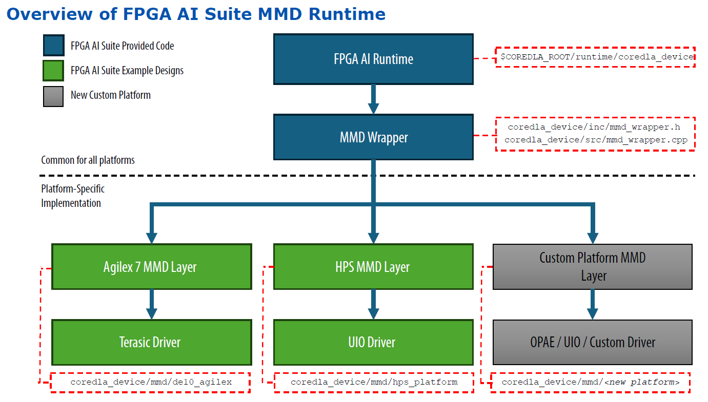
The interface to the user-space portion of the BSP drivers is centralized in the MmdWrapper class, which can be found in the file $COREDLA_ROOT/runtime/coredla_device/inc/mmd_wrapper.h. This file is a wrapper around the MMD API.
The FPGA AI Suite runtime uses this wrapper so that the runtime can be reused on all platforms. When porting the runtime to a new board, you must ensure that each of the member functions in MmdWrapper calls into a board-specific implementation function. You must also modify the runtime build process and adjacent code.
Any implementation of a runtime for the FPGA AI Suite must support the following features via the MMD Wrapper:
- Open the device
- Register an interrupt service routine
- Read/write 32-bit register values in the IP control-and-status register (CSR)
- Transfer bulk data between the host and device
3.3.5. Memory-Mapped Device (MMD) Driver
The FPGA AI Suite runtime MMD software uses a driver to access and interact with the FPGA device. To integrate the FPGA AI Suite IP into your design on your platform, the MMD layer must interface with the hardware using the appropriate drivers (such as OPAE, UIO, or a custom driver). For example, the PCIe-based design example uses the drivers provided by the OpenCL board support package (BSP) for the Terasic DE10-Agilex Development Board.
If your board vendor provides a BSP, you can use the MMD Wrapper to interface the BSP with the FPGA AI Suite IP. Review the following sections for examples of adapting a vendor-provided BSP to use with the FPGA AI Suite IP:
You can create a custom BSP for your board, but that process can be complex and can require more work.
The FPGA AI Suite runtime MMD software uses a driver to access and interact with the FPGA device. This driver is supplied as part of the board vendor BSP or, for OFS-based boards, the OPAE driver.
The source files for the MMD driver are provided in runtime/coredla_device/mmd. The source files contain classes for managing and accessing the FPGA device by using driver-supplied functions for reading/writing to CSR, reading/writing to DDR, and handling kernel interrupts.
Obtaining BSP Drivers
Contact your FPGA board vendor for information about the BSP for your FPGA board.
Obtaining the OPAE Drivers
Contact your FPGA board vendor for information about the OPAE driver for your FPGA board.
For the FPGA AI Suite OFS for PCIe attach design example, the OPAE driver is installed when you follow the steps in Getting Started with Open FPGA Stack (OFS) for PCIe-Attach Design Examples.
3.3.6. FPGA AI Suite Runtime MMD API
This section describes board-level functions that are defined in the mmd_wrapper.cpp file. Your implementation of the functions in the mmd_wrapper.cpp file for your specific board may differ. For examples of these functions, refer to the provided MMD implementations under $COREDLA_ROOT/runtime/coredla_device/mmd/.
The mmd_wrapper.cpp file contains the following MMD functions that are adapted from the Open FPGA Stack (OFS) accelerator support package (ASP) functions of the same name. For more information about these functions, refer to the OFS AFS Memory Mapped Device Layer documentation.
Although several of the functions in the FPGA AI Suite MMD API share names and intended behavior with OpenCL MMD API functions, you do not need to use an OpenCL BSP. The naming convention is maintained for historical reasons only.
The mmd_wrapper.cpp file contains the following functions provided only with the FPGA AI Suite:
- dla_mmd_get_max_num_instances
- dla_mmd_get_ddr_size_per_instance
- dla_mmd_get_coredla_clock_freq
- dla_mmd_get_ddr_clock_freq
- dla_mmd_csr_read
- dla_mmd_csr_write
- dla_mmd_ddr_read
- dla_mmd_ddr_write
- dla_is_stream_controller_valid
- dla_mmd_stream_controller_read
- dla_mmd_stream_controller_write
The dla_mmd_get_max_num_instances Function
Returns the maximum number of FPGA AI Suite IP instances that can be instantiated on the platform. In the FPGA AI Suite PCIe-based design examples, this number of IP instances that can be instantiated is the same as the number of external memory interfaces (for example, DDR memories).
Syntax
The dla_mmd_get_ddr_size_per_instance Function
Returns the maximum amount of external memory available to each FPGA AI Suite IP instance.
Syntax
The dla_mmd_get_coredla_clock_freq Function
Given the device handle, return the FPGA AI Suite IP PLL clock frequency in MHz. Return a negative value if there is an error.
In the PCIe-based design example, this value is determined by allowing a set amount of wall clock time to elapse between reads of counters onboard the IP.
Syntax
The dla_mmd_get_ddr_clock_freq Function
Returns the DDR clock frequency, in Mhz. Check the documentation from your board vendor to determine this value.
Syntax
The dla_mmd_csr_read Function
Performs a control status register (CSR) read for a given instance of the FPGA AI Suite IP at a given address. The result is stored in the data directory.
Syntax
The dla_mmd_csr_write Function
Performs a control status register (CSR) write for a given instance of the FPGA AI Suite IP at a given address.
Syntax
The dla_mmd_ddr_read Function
Performs an external memory read for a given instance of the FPGA AI Suite IP at a given address. The result is stored in the data directory.
Syntax
The dla_mmd_ddr_write Function
Performs an external memory write for a given instance of the FPGA AI Suite IP at a given address.
Syntax
The dla_is_stream_controller_valid Function
Optional. Required if STREAM_CONTROLLER_ACCESS is defined.
Queries the streaming controller device to see if it is valid.
Syntax
For more information about the stream controller module, refer to [SOC] Stream Controller Communication Protocol.
The dla_mmd_stream_controller_read Function
Optional. Required if STREAM_CONTROLLER_ACCESS is defined.
Reads an incoming message from the streaming controller.
Syntax
int dla_mmd_stream_controller_read(int handle, int instance, uint64_t addr, uint64_t length, void* data)
For more information about the streaming controller device, refer to [SOC] Stream Controller Communication Protocol.
The dla_mmd_stream_controller_write Function
Optional. Required if STREAM_CONTROLLER_ACCESS is defined.
Writes an outgoing message from the streaming controller.
Syntax
int dla_mmd_stream_controller_write(int handle, int instance, uint64_t addr, uint64_t length, const void* data)
For more information about the streaming controller device, refer to [SOC] Stream Controller Communication Protocol.
3.3.7. Board Support Package (BSP) Overview
Every FPGA platform consists of the FPGA fabric and the hard IP that surrounds it. For example, an FPGA platform might provide an external memory interface as hard IP to provide access to external DDR memory. Soft logic that is synthesized on the FPGA fabric needs to be able to communicate with the hard IP blocks, and the implementation details are typically platform-specific.
A board support package (BSP) typically consists of two parts:
- A software component that runs in the host operating system.
This component includes the MMD and operating system driver for the board.
- A hardware component that is programming into the FPGA fabric.
This component consists of soft logic that enables the use of the FPGA peripheral hard IP blocks around the FPGA fabric. This component acts as the bridge between the FPGA AI Suite IP block in the FPGA fabric and the hard IP blocks.
Depending on your board and board vendor, you can have the following options for obtaining a BSP:
- If your board supports the Open FPGA Stack (OFS), you can use (and adapt, if necessary) an OFS reference design or FPGA interface manager (FIM).
For some boards, there are precompiled FIM reference designs available.
- Obtain a BSP directly from your board vendor. You board vendor might have multiple BSPs available for you board.
- Create your own BSP.
For a BSP to be compatible with FPGA AI Suite, the BSP must provide the following capabilities:
- Enable the FPGA AI Suite IP and the host to interface with the external memory interface IP.
- Enable the FPGA AI Suite IP to interface with the runtime (for example, PCIe IP for the PCIe-based design example, or the HPS-to-FPGA AXI bridge for the SoC design example).
- Enable the FPGA AI Suite IP to send interrupts to the runtime. If your BSP does not support this capability, you must use polling to determine when an inference is complete.
- Enable the host to access the FPGA AI Suite IP CSR.
The BSPs available for the boards supported by the FPGA AI Suite design example support these capabilities.
Related Information
Open FPGA Stack (OFS) documentation.
3.3.7.1. Terasic DE10-Agilex™ Development Board BSP Example
For the Agilex™ 7 PCIe-based design example on the Terasic DE10-Agilex Development Board, the BSP provided by Terasic is adapted to work with the FPGA AI Suite IP. The Terasic-provided BSP is OpenCL™-based.
The following diagram shows the high-level interactions between the FPGA interface IPs on the platform, and the a custom OpenCL kernel. The different colors in the diagram indicate different clock domains.
Figure 3. Terasic BSP with OpenCL Kernel
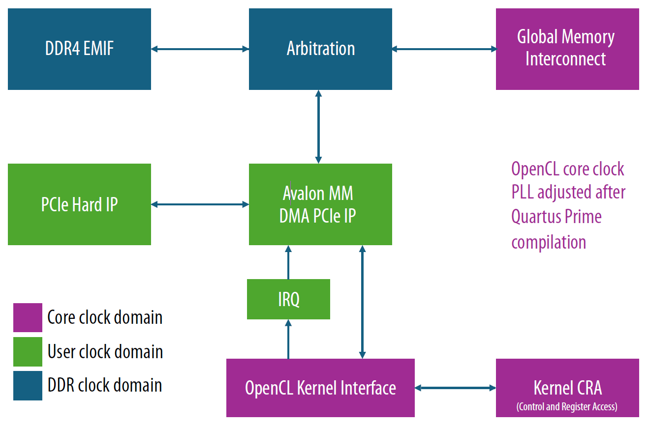
The PCIe hard IP can read/write to the DDR4 external memory interface (EMIF) via the DMA and the Arbitrator. Additional logic is provided to handle interrupts from the custom IP and propagate them back to the host through the PCIe interface.
The following diagram hows how the Terasic DE10-Agilex Development Board BSP can be adapted to support the FPGA AI Suite IP.
Figure 4. Terasic BSP With FPGA AI Suite IP
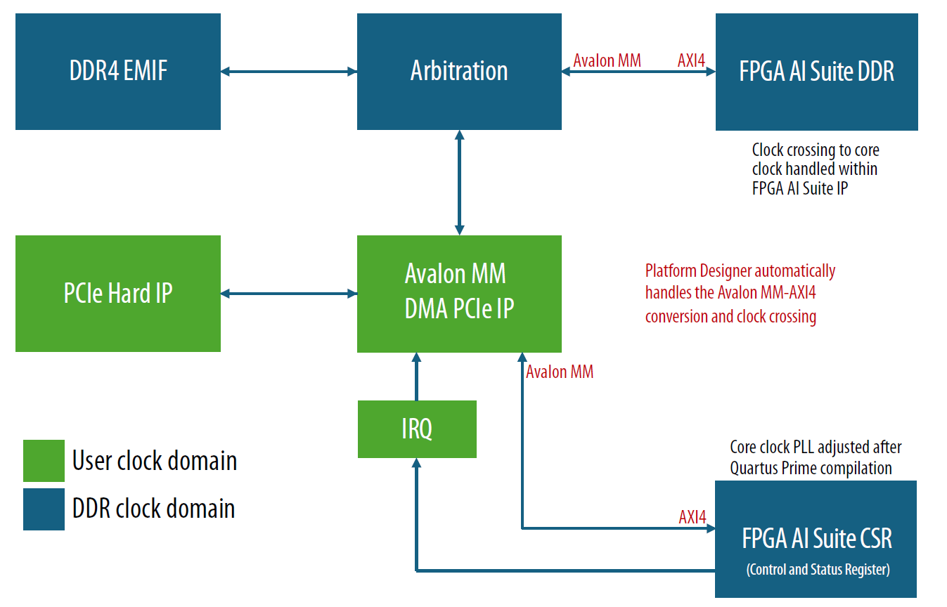
Platform Designer automatically adds clock-domain crossings between Avalon memory-mapped interfaces and AXI4 interfaces, making the integration with the BSP easier.
For a custom platform, consider following a similar approach of modifying the BSP provided by the vendor to integrate in the FPGA AI Suite IP.
3.3.7.2. Agilex™ 7 PCIe-Attach OFS-based BSP Example
For OFS-based devices, the BSP consists of a platform-specific FPGA interface manager (FIM) and a platform-agnostic accelerator functional unit (AFU).
The FPGA AI Suite OFS for PCIe attach design example supports Agilex™ 7 PCIe Attach OFS.
You can obtain the source files needed to build a Agilex™ 7 PCIe Attach FIM or obtain prebuillt FIMs for some boards from OFS Agilex™ 7 PCIe Attach FPGA Development Directory in GitHub.
The AFU wraps the FPGA AI Suite IP and must meet the following general requirements:
- The AFU must include an instance of the FPGA AI Suite IP.
- The AFU must support host access (for example, via DMA) to external memory that is shared with the FPGA AI Suite IP.
- The AFU must propagate interrupts from the FPGA AI Suite IP to the host.
- The AFU Must support host access to the FPGA AI Suite IP CSR memory.
If you are creating your own FPGA AI Suite AFU, consider starting with an AFU example design that implements some of the required functionality. Some examples designs and what they are offer are as follows:
- For an example of enabling direct memory access so the host can access DDR memory, review the direct memory access (DMA) AFU example on GitHub
- For an example of interrupt handling, review the oneAPI Accelerator Support Package (ASP) on GitHub.
- For an example MMD implementation, review the oneAPI Accelerator Support Package (ASP) on GitHub.
Related Information
- Direct memory access (DMA) AFU example on GitHub
- oneAPI accelerator support package (ASP) on GitHub
- Agilex™ 7 PCIe Attach OFS documentation
- Agilex™ 7 PCIe Attach OFS Workload Development Guide
4.0 Getting Started with the FPGA AI Suite PCIe-based Design Example
Before starting with the FPGA AI Suite PCIe-based Design Example, ensure that you have followed all the installation instructions for the FPGA AI Suite compiler and IP generation tools and completed the design example prerequisites as provided in the FPGA AI Suite Handbook.
The FPGA AI Suite PCIe-attach design example (sometimes referred to as the PCIe-based design example) demonstrates how the Intel Distribution of OpenVINO toolkit and the FPGA AI Suite support the look-aside deep learning acceleration model.
The PCIe-attach design example is implemented with the following components:
- FPGA AI Suite IP
- Intel Distribution of OpenVINO toolkit
- Terasic DE10-Agilex Development Board
- Sample hardware and software systems that illustrate the use of these components
This design example includes prebuilt FPGA bitstreams that correspond to preoptimized architecture files. However, the design example build scripts let you choose from a variety of architecture files and build (or rebuild) your own bitstreams, provided that you have a license permitting bitstream generation.
This design is provided with the FPGA AI Suite as an example showing how to incorporate the IP into a design. This design is not intended for unaltered use in production scenarios. Any potential production application that uses portions of this example design must review them for both robustness and security.
5.0 Building the FPGA AI Suite Runtime
The FPGA AI Suite PCIe-based Design Example runtime directory contains the source code for the OpenVINO plugins and customized versions of the following OpenVINO programs:
dla_benchmarkclassification_sample_asyncobject_detection_demo_yolov3_asyncsegmentation_demo
The CMake tool manages the overall build flow to build the FPGA AI Suite runtime plugin.
5.1 CMake Targets
The top level CMake build target is the FPGA AI Suite runtime plugin shared library, libcoreDLARuntimePlugin.so. It will not be built if the target is the software reference. Details on how to target one of the example design boards or the software emulation are specified in Build Options. The source files used to build the libcoreDLARuntimePlugin.so target are located under the following directories:
runtime/plugin/src/runtime/coredla_device/src/
The flow also builds additional targets as dependencies for the top-level target. The most significant additional targets are as follows:
- The Input and Output Layout Transform library,
libdliaPluginIOTransformations.a. The sources for this target are underruntime/plugin/io_transformations/.
5.2 Build Options
The runtime folder in the design example package contains a script to build the runtime called build_runtime.sh.
Issue the following command to run the script:
Where \<command_line_options> are defined in the following table:
Table 1: Command Line Options for the build_runtime.sh Script
| Command | Description |
|---|---|
| -h | --help |
| --cmake_debug | Call cmake with a debug flag |
| --verbosity=<number> | Large numbers add some extra verbosity |
| --build_dir=<path> | Directory where the runtime build should be placed |
| --disable_jit | If this flag is specified, then the runtime will only support the Ahead of Time mode. The runtime will not link to the precompiled compiler libraries. Use this mode when trying to compile the runtime on an unsupported operating system. |
| --build_demo | Adds several OpenVINO demo applications to the runtime build. The demo applications are in subdirectories of the runtime/directory. |
| --target_de10_agilex | Target the Terasic DE10-Agilex Development Board. |
| --target_emulation | Target the software emulator model. Specify this option to build the runtime without a board installed. Inference requests are executed by the software emulator model of the FPGA AI Suite IP. |
| --aot_splitter_example | Builds the AOT splitter example utility for the selected target (Terasic DE10-Agilex Development Board). This option builds an AOT file for a model, splits the AOT file into its constituent components (weights, overlay instructions, etc), and the builds a small utility that loads the model and a single image onto the target FPGA board without using OpenVINO. You must set the $AOT_SPLITTER_EXAMPLE_MODEL and $AOT_SPLITTER_EXAMPLE_INPUT environment variables correctly. For details, refer to "FPGA AI Suite Ahead-of-Time (AOT) Splitter Utility Example Application" in FPGA AI Suite Handbook. |
The FPGA AI Suite runtime plugin is built in release mode by default. To enable debug mode, you must specify the --cmake_debug option of the script command.
The -no_make option skips the final call to the make command. You can make this call manually instead.
FPGA AI Suite hardware is compiled to include one or more IP instances, with the same architecture for all instances. Each instance accesses data from a unique bank of DDR:
- The Terasic DE10-Agilex Development Board has four DDR banks and supports up to four instances.
The runtime automatically adapts to the correct number of instances.
If the FPGA AI Suite runtime uses two or more instances, then the image batches are divided between the instances to execute two or more batches in parallel on the FPGA device.
6.0 Running the Design Example Demonstration Applications
This section describes the steps to run the demonstration application and perform accelerated inference using the PCIe Example Design.
6.1 Exporting Trained Graphs from Source Frameworks
Before running any demonstration application, you must convert the trained model to the Inference Engine format (.xml, .bin) with the OpenVINO Model Optimizer.
For details on creating the .bin/.xml files, refer to the FPGA AI Suite Handbook.
6.2 Compiling Exported Graphs Through the FPGA AI Suite
The network as described in the .xml and .bin files (created by the Model Optimizer) is compiled for a specific FPGA AI Suite architecture file by using the FPGA AI Suite compiler.
The FPGA AI Suite compiler compiles the network and exports it to a .bin file that uses the same .bin format as required by the OpenVINO Inference Engine.
This .bin file created by the compiler contains the compiled network parameters for all the target devices (FPGA, CPU, or both) along with the weights and biases. The inference application imports this file at runtime.
The FPGA AI Suite compiler can also compile the graph and provide estimated area or performance metrics for a given architecture file or produce an optimized architecture file.
For more details about the FPGA AI Suite compiler, refer to the FPGA AI Suite Handbook.
6.3 Compiling the PCIe-based Example Design
Prepackaged bitstreams are available for the PCIe Example Design. If the prepackaged bitstreams are installed, they are installed in demo/bitstreams/.
To build example design bitstreams, you must have a license that permits bitstream generation for the IP, and have the correct version of Quartus Prime software installed.
Use the dla_build_example_design.py utility to create a bitstream.
For details about this command, the steps it performs, and advanced command options, refer to The dla_build_example_design.py and to the FPGA AI Suite Handbook.
6.4 Programming the FPGA Device (Agilex 7)
You can program the Terasic DE10-Agilex Development Board board using the fpga_jtag_reprogram tool.
For details, refer to "FPGA AI Suite Quick Start Tutorial" in the FPGA AI Suite Handbook.
6.5 Performing Accelerated Inference with the dla_benchmark Application
You can use the dla_benchmark demonstration application included with the FPGA AI Suite runtime to benchmark the performance of image classification networks.
6.5.1 Inference on Image Classification Graphs
The demonstration application requires the OpenVINO device flag to be either HETERO:FPGA,CPU for heterogeneous execution or HETERO:FPGA for FPGA-only execution.
The dla_benchmark demonstration application runs five inference requests (batches) in parallel on the FPGA, by default, to achieve optimal system performance. To measure steady state performance, you should run multiple batches (using the -niter flag) because the first iteration is significantly slower with FPGA devices.
The dla_benchmark demonstration application also supports multiple graphs in the same execution. You can place more than one graphs or compiled graphs as input, separated by commas.
Each graph can have either a different input dataset or use a commonly shared dataset among all graphs. Each graph requires an individual ground_truth_file file, separated by commas. If some ground_truth_file files are missing, the dla_benchmark continues to run and ignore the missing ones.
When multi-graph is enabled, the -niter flag represents the number of iterations for each graph, so the total number of iterations becomes -niter × number of graphs.
The dla_benchmark demonstration application switches graphs after submitting -nireq requests. The request queue holds the number of requests up to -nireq × number of graphs. This limit is constrained by the DMA CSR descriptor queue size (64 per hardware instance).
The board you use determines the number of instances that you can compile the FPGA AI Suite hardware for:
- For the Terasic DE10-Agilex Development Board, you can compile up to four instances with the same architecture on all instances.
Each instance accesses one of the DDR banks on the board and executes the graph independently. This optimization enables multiple batches to run in parallel, limited by the number of DDR banks available. Each inference request created by the demonstration application is assigned to one of the instances in the FPGA plugin.
To enable memory-mapped device (MMD) debug messages when you run the dla_benchmark demonstration application. set the ACL_PCIE_DEBUG environment variable as follows:
Also, you can test full DDR write and read back functionality when the dla_benchmark demonstration application runs by setting the COREDLA_RUNTIME_MEMORY_TEST environment variable as follows:
To ensure that batches are evenly distributed between the instances, you must choose an inference request batch size that is a multiple of the number of FPGA AI Suite instances. For example, with two instances, specify the batch size as six (instead of the OpenVINO default of five) to ensure that the experiment meets this requirement.
The example usage that follows has the following assumptions:
- A Model Optimizer IR
.xmlfile is indemo/models/public/resnet-50-tf/FP32/ - An image set is in
demo/sample_images/ - The board is programmed with a bitstream that corresponds to
AGX7_Performance.arch
binxml=$COREDLA_ROOT/demo/models/public/resnet-50-tf/FP32

imgdir=$COREDLA_ROOT/demo/sample_images

cd $COREDLA_ROOT/runtime/build_Release
./dla_benchmark/dla_benchmark \
-b=1 \
-m $binxml/resnet-50-tf.xml \
-d=HETERO:FPGA,CPU \
-i $imgdir \
-niter=4 \
-plugins ./plugins.xml \
-arch_file $COREDLA_ROOT/example_architectures/AGX7_Performance.arch \
-api=async \
-groundtruth_loc $imgdir/TF_ground_truth.txt \
-perf_est \
-nireq=8 \
-bgr
The following example shows how the FPGA AI Suite IP can dynamically swap between graphs. This example usage assumes that another Model Optimizer IR .xml file has been placed in demo/models/public/resnet-101-tf/FP32/. It also assumes that another image set has been placed into demo/sample_images_rn101/. In this case, dla_benchmark only evaluates the classification accuracy of Resnet50 because we did not provide ground truth for the second graph (ResNet101).
binxml1=$COREDLA_ROOT/demo/models/public/resnet-50-tf/FP32

binxml2=$COREDLA_ROOT/demo/models/public/resnet-101-tf/FP32

imgdir1=$COREDLA_ROOT/demo/sample_images

imgdir2=$COREDLA_ROOT/demo/sample_images_rn101

cd $DEVELOPER_PACKAGE_ROOT/runtime/build_Release
./dla_benchmark/dla_benchmark \
-b=1 \
-m $binxml1/resnet-50-tf.xml,$binxml2/resnet-101-tf.xml \
-d=HETERO:FPGA,CPU \
-i $imgdir1,$imgdir2 \
-niter=8 \
-plugins ./plugins.xml \
-arch_file $COREDLA_ROOT/example_architectures/AGX7_Performance.arch \
-api=async \
-groundtruth_loc $imgdir1/TF_ground_truth.txt \
-perf_est \
-nireq=8 \
-bgr
6.5.2 Inference on Object Detection Graphs
To enable the accuracy checking routine for object detection graphs, you can use the -enable_object_detection_ap=1 flag.
This flag lets the dla_benchmark calculate the mAP and COCO AP for object detection graphs. Besides, you need to specify the version of the YOLO graph that you provide to the dla_benchmark through the –yolo_version flag. Currently, this routine is known to work with YOLOv3 (graph version is yolo-v3-tf) and TinyYOLOv3 (graph version is yolo-v3-tiny-tf).
6.5.2.1 The mAP and COCO AP Metrics
Average precision and average recall are averaged over multiple Intersection over Union (IoU) values.
Two metrics are used for accuracy evaluation in the dla_benchmark application. The mean average precision (mAP) is the challenge metric for PASCAL VOC. The mAP value is averaged over all 80 categories using a single IoU threshold of 0.5. The COCO AP is the primary challenge for object detection in the Common Objects in Context contest. The COCO AP value uses 10 IoU thresholds of .50:.05:.95. Averaging over multiple IoUs rewards detectors with better localization.
6.5.2.2 Specifying Ground Truth
The path to the ground truth files is specified by the flag –groundtruth_loc.
The validation dataset is available on the COCO official website.
The dla_benchmark application currently allows only plain text ground truth files. To convert the downloaded JSON annotation file to plain text, use the convert_annotations.py script.
6.5.2.3 Example of Inference on Object Detection Graphs
The example that follows makes the following assumptions:
- The Model Optimizer IR
graph.xmlfor either YOLOv3 or TinyYOLOv3 is in the current working directory.
Model Optimizer generates an FP32 version and an FP16 version. Use the FP32 version.
- The validation images downloaded from the COCO website are placed in the
./mscoco-imagesdirectory.
- The JSON annotation file is downloaded and unzipped in the current directory.
To compute the accuracy scores on many images, you can usually increase the number of iterations using the flag -niter instead of a large batch size -b. The product of the batch size and the number of iterations should be less than or equal to the number of images that you provide.
cd $COREDLA_ROOT/runtime/build_Release

python ./convert_annotations.py ./instances_val2017.json \
./groundtruth
./dla_benchmark/dla_benchmark \
-b=1 \
-niter=5000 \
-m=./graph.xml \
-d=HETERO:FPGA,CPU \
-i=./mscoco-images \
-plugins=./plugins.xml \
-arch_file=../../example_architectures/AGX7_Performance.arch \
-yolo_version=yolo-v3-tf \
-api=async \
-groundtruth_loc=./groundtruth \
-nireq=8 \
-enable_object_detection_ap \
-perf_est \
-bgr
6.5.3 Additional dla_benchmark Options
The dla_benchmark tool is part of the example design and the distributed runtime includes full source code for the tool.
Table 2: Command Line dla_benchmark Options
| Command Option | Description |
|---|---|
| -nireq=<N> | This option controls the number of simultaneous inference requests that are sent to the FPGA. Typically, this should be at least twice the number of IP instances; this ensures that each IP can execute one inference request while dla_benchmark loads the feature data for a second inference request to the FPGA-attached DDR memory. |
| -b=<N> --batch-size=<N> |
This option controls the batch size. A batch size greater than 1 is created by repeating configuration data for multiple copies of the graph. A batch size of 1 is typically best for latency System throughput for small graphs, when inference operations are offloaded from a CPU to an FPGA, may improve by using a batch greater than 1. On very small graphs, IP throughput may also improve when using a batch greater than 1. The default value is 1. |
| -niter=<N> | Number of batches to run. Each batch has a size specified by the --batch-size option. The total number of images processed is the product of the --batch-size option value multiplied by the -niter option value. |
| -d=<STRING> | Using -d=HETERO:FPGA, CPU causes dla_benchmark to use the OpenVINO heterogeneous plugin to execute inference on the FPGA, with fallback to the CPU for any layers that cannot go to the FPGA. Using -d=HETERO:CPU or -d=CPU executes inference on the CPU, which may be useful for testing the flow when an FPGA is not available. Using -d=HETERO:FPGA may be useful for ensuring that all graph layers are accelerated on the FPGA (and an error is issued if this is not possible). |
| -arch_file=<FILE> --arch=<FILE> |
This specifies the location of the .arch file that was used to configure the IP on the FPGA. The dla_benchmark will issue an error if this does not match the.arch file used to generate the IP on the FPGA. |
| -m=<FILE> --network_file=<FILE> |
This points to the XML file from OpenVINO Model Optimizer that describes the graph. The BIN file from Model Optimizer must be kept in the same directory and same filename (except for the file extension) as the XML file. |
| -i=<DIRECTORY> | This points to the directory containing the input images. Each input file corresponds to one inference request. The files are read in order sorted by filename; set the environment variable VERBOSE=1 to see details describing the file order. |
| -api=[sync|async] | The -api=async option allows dla_benchmark to fully take advantage of multithreading to improve performance. The -api=sync option may be used during debug. |
| -groundtruth_loc=<FILE> | Location of the file with ground truth data. If not provided, then dla_benchmark will not evaluate accuracy. This may contain classification data or object detection data, depending on the graph. |
| -yolo_version=<STRING> | This option is used when evaluating the accuracy of a YOLOv3 or TinyYOLOv3 object detection graph. The options are yolo-v3-tf and yolo-v3-tiny-tf. |
| -enable_object_detection_ap | This option may be used with an object detection graph (YOLOv3 or TinyYOLOv3) to calculate the object detection accuracy. |
| -bgr | When used, this flag indicates that the graph expects input image channel data to use BGR order. |
| -plugins_xml_file=<FILE> | Deprecated: This option is deprecated and will be removed in a future release. Use the -plugins option instead. This option specifies the location of the file specifying the OpenVINO plugins to use. This should be set to $COREDLA_ROOT/runtime/plugins.xml in most cases. If you are porting the design to a new host or doing other development, it may be necessary to use a different value. |
| -plugins=<FILE> | This option specifies the location of the file that specifies the OpenVINO plugins to use. The default behavior is to read the plugins.xml file from the runtime/ directory. This runs inference on the FPGA device. If you want to run inference using the emulation model, specify -plugins=emulation. If you are porting the design to a new host or doing other development, you might need to use a different value. |
| -mean_values=<input_name[mean_values]> | Uses channel-specific mean values in input tensor creation through the following formula: ((input − mean) / scale) . The Model Optimizer mean values are the preferred choice and the mean values defined by this option serve as fallback values. |
| -scale_values=<input_name[scale_values]> | Uses channel-specific scale values in input tensor creation through the following formula: ((input − mean) / scale) . The Model Optimizer scale values are the preferred choice and the scale values defined by this option serve as fallback values. |
| -pc | This option reports the performance counters for the CPU subgraphs, if there is any. No sorting is done on the report. |
| -pcsort=[sort|no_sort|simple_sort] | This option reports the performance counters for the CPU subgraph and sets the sorting option for the performance counter report: * sort: Report is sorted by operation time cost \n* no_sort: Report is not sorted \n* simple_sort: Report is sorted by opts time cost but print only executed operations |
| -save_run_summary | Collect performance metrics during inference. These metrics can help you determine how efficient an architecture is at executing a model. For more information, refer to The dla_benchmark Performance Metrics |
6.5.4 The dla_benchmark Performance Metrics
The -save_run_summary option makes the dla_benchmark demonstration application collect performance metrics during inference. These metrics can help you determine how efficient an architecture is at executing a model.
Note: The dla_benchmark application provides throughput in "frames per second". The time per frame (latency) is 1/throughput.
| Statistic | Description |
|---|---|
| Count | The number of times interference was performed. This is set by the -niter option. |
| System duration | The total time between when the first inference request was made to when the last request was finished, as measured by the host program. |
| IP duration | The total time the spent-on inference. This is reported by the IP on the FPGA. |
| Latency | The median time of all inference requests made by the host. This includes any overhead from OpenVINO or the FPGA AI Suite runtime. |
| System throughput | The total throughput of the system, including any OpenVINO or FPGA AI Suite runtime overhead. |
| Number of hardware instances | The number of IP instances on the FPGA. |
| Number of network instances | The number graphs that the IP processes in parallel. |
| IP throughput per instance | The throughput of a single IP instance. This is reported by the IP on the FPGA. |
| IP throughput per fMAX per instance | The IP throughput per instance value scaled by the IP clock frequency value. |
| IP clock frequency | The clock frequency, as reported by the IP running on the FPGA device. The dla_benchmark application treats this value as the IP core fMAX value. |
| Estimated IP throughput per instance | The estimated per-IP throughput, as estimated by the dla_compiler command with the --fanalyze-performance option. |
| Estimated IP throughput per fmax per instance | The Estimated IP throughput per instance value scaled by the compiler fMAX estimate. |
6.5.4.1 Interpreting System Throughput and Latency Metrics
The System throughput and Latency metrics are measured by the host through the OpenVINO API. These measurements include any overhead that is incurred by both the API and the FPGA AI Suite runtime. They also account for any time spent waiting to make inference requests and the number of available instances.
In general, the system throughput is defined as follows:
The Batch Size and Images Per Batch values are set by the --batch-size and -niter options, respectively.
For example, consider when -nireq=1 and there is a single IP instance. The System throughput value is approximately the same as the IP-reported throughput value because the runtime can perform only one inference at a time. However, if both the -nireq and the number of IP instances is greater than one, the runtime can perform requests in parallel. As such, the total system throughput is greater than the individual IP throughput.
In general, the -nireq value should be twice the number of IP instances. This setting enables the FPGA AI Suite runtime to pipeline inferences requests, which allows the host to prepare the data for the next request while an IP instance is processing the previous request.
6.6 Running the Ported OpenVINO Demonstration Applications
Some of the sample demonstration applications from the OpenVINO toolkit for Linux Version 2024.6 have been ported to work with the FPGA AI Suite. These applications are built at the same time as the runtime when using the -build_demo flag to build_runtime.sh.
The FPGA AI Suite runtime includes customized versions of the following demo applications for use with the FPGA AI Suite IP and plugins:
classification_sample_asyncobject_detection_demo_yolov3_asyncsegmentation_demo
Each demonstration application uses a different graph. The OpenVINO HETERO plugin can fall-back to the CPU for portions of the graph that are not supported with FPGA-based acceleration. However, in a production environment, it may be more efficient to use alternate graphs that execute exclusively on the FPGA.
You can use the example .arch files that are supplied with the FPGA AI Suite with the demonstration applications. However, certain example .arch files do not enable some of the layer-types used by the graphs associated with the demonstration applications. Using these .arch files cause portions of the graph to needlessly execute on the CPU.
To minimize the number of layers that are executed on the CPU by the demonstration application, use the following architecture description files located in the example_architectures/ directory of the FPGA AI Suite installation package to run the demos:
- Agilex 7:
AGX7_Generic.arch
As specified in Programming the FPGA Device (Agilex 7), you must program the FPGA device with the bitstream for the architecture being used. Each demonstration application includes a README.md file specifying how to use it.
When the OpenVINO sample applications are modified to support the FPGA AI Suite, the FPGA AI Suite plugin used by OpenVINO needs to know how to find the .arch file describing the IP parameterization by using the following configuration key. The following C++ code is used in the demo for this purpose:
The OpenVINO demonstration application hello_query_device does not work with the FPGA AI Suite due to low-level hardware identification assumptions.
6.6.1 Example Running the Object Detection Demonstration Application
You must download the following items:
yolo-v3-tffrom the OpenVINO Model Downloader. The command should look similar to the following command:
python3 <path_to_installation>/open_model_zoo/omz_downloader \
--name yolo-v3-tf \
--output_dir <download_dir>
From the downloaded model, generate the .bin/.xml files:
python3 <path_to_installation>/open_model_zoo/omz_converter \
--name yolo-v3-tf \
--download_dir <download_dir> \
--output_dir <output_dir> \
--mo <path_to_installation>/model_optimizer/mo.py
Model Optimizer generates an FP32 version and an FP16 version. Use the FP32 version.
- Input video from: https://github.com/intel-iot-devkit/sample-videos.
- The recommended video is
person-bicycle-car-detection.mp4
To run the object detection demonstration application,
- Ensure that demonstration applications have been built with the following command:
-
Ensure that the FPGA has been configured with the Generic bitstream.
-
Run the following command:
./runtime/build_Release/object_detection_demo/object_detection_demo \
-d HETERO:FPGA,CPU \
-i <path_to_video>/input_video.mp4 \
-m <path_to_model>/yolo_v3.xml \
-arch_file=$COREDLA_ROOT/example_architectures/AGX7_Generic.arch \
-plugins $COREDLA_ROOT/runtime/plugins.xml \
-t 0.65 \
-at yolo
Tip: High-resolution video input, such as when using HD camera as input, imposes considerable decoding overhead on the inference engine that can potentially lead to reduced system throughput. Use the the -input_resolution=<width>x<height> option that is included in the demonstration application to adjust the input resolution to a level that balances video quality with system performance.
7.0 Design Example System Architecture for the Agilex 7 FPGA
The Agilex 7 design example is derived from the BSP provided by the Terasic DE10-Agilex Development Board.
7.1 System Overview
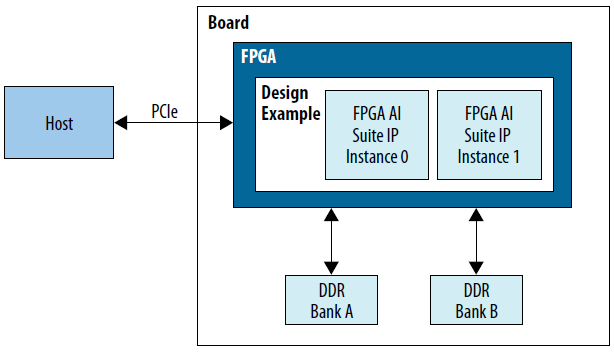
The system consists of the following components connected to a host system via a PCIe interface as shown in the following figure.
- A board with the FPGA device
- On-board DDR memory
The FPGA image consists of the FPGA AI Suite IP and an additional logic that connects it to a PCIe interface and DDR. The host can read and write to the DDR memory through the PCIe port. In addition, the host can communicate and control the FPGA AI Suite instances through the PCIe connection which is also connected the direct memory access (DMA) CSR port of FPGA AI Suite instances.
The FPGA AI Suite IP accelerates neural network inference on batches of images. The process of executing a batch follows these steps:
- The host writes a batch of images, weights, and configuration data to DDR where weights can be reused between batches.
- The host writes to the FPGA AI Suite CSR to start execution.
- FPGA AI Suite computes the results of the batch and stores them in DDR.
- Once the computation is complete, FPGA AI Suite raises an interrupt to the host.
- The host reads back the results from DDR.
Figure 1: FPGA AI Suite Example Design System Overview
7.2 Hardware
This section describes the PCIe-based Example Design in detail.
A top-level view of the design example is shown in FPGA AI Suite Example Design Top Level.
The instances of FPGA AI Suite IP are on the right (dla_top.sv). All communication between the FPGA AI Suite IP systems and the outside occurs via the FPGA AI Suite IP DMA. The FPGA AI Suite IP DMA provides a CSR (which also has interrupt functionality) and reader/writer modules which read/write from DDR.
The host communicates with the board through the PCIe protocol. The host can do the following things:
- Read and write the on-board DDR memory (these reads/writes do not go through FPGA AI Suite IP).
- Read/write to the FPGA AI Suite IP DMA CSR of the instances.
- Receive interrupt signals from the FPGA AI Suite IP DMA CSR of both instances.
Each FPGA AI Suite IP instance can do the following things:
- Read/write to its DDR bank.
- Send interrupts to the host through the interrupt interface.
- Receive reads/writes to its DMA CSR.
From the perspective of the FPGA AI Suite, external connections are to the PCIe interface and to the on-board DDR4 memory. The DDR memory is connected directly to mem.qsys block, while the PCIe interface is converted into Avalon® memory mapped (MM) interfaces in pcie_ed.qsys block for communication with the mem.qsys block.
The mem.qsys blocks arbitrate the connections to DDR memory between the reader/writer modules in FPGA AI Suite IP and reads/writes from the host. Each FPGA AI Suite IP instance in this design has access to only one of the DDR banks. This design decision implies that the number simultaneous FPGA AI Suite IP instances that can exist in the design is limited to the number of DDR blocks available on the board. Adding an additional arbiter would relax this restriction and allow additional FPGA AI Suite IP instances.
Much of board.qsys operates using the Avalon Memory-mapped (MM) interface protocol. The FPGA AI Suite DMA uses AXI protocol, and board.qsys has Avalon MM interface to AXI adapters just before each interface is exported to the FPGA AI Suite IP (so that outside of the Platform Designer system it can be connected to FPGA AI Suite IP). Clock crossing is also handled inside of board.qsys. For example, the host interface must be brought to the DDR clock to talk with the FPGA AI Suite IP CSR.
There are three clock domains: host clock, DDR clock, and the FPGA AI Suite IP clock. The PCIe logic runs on the host clock. FPGA AI Suite DMA and the platform adapters run on the DDR clock. The rest of FPGA AI Suite IP runs on the FPGA AI Suite IP clock.
FPGA AI Suite IP protocols:
- Readers and Writers: 512-bit data (width configurable), 32-bit address AXI4 interface, 16-word max burst (width fixed).
- CSR: 32-bit data, 11-bit address
Figure 2: FPGA AI Suite Example Design Top Level
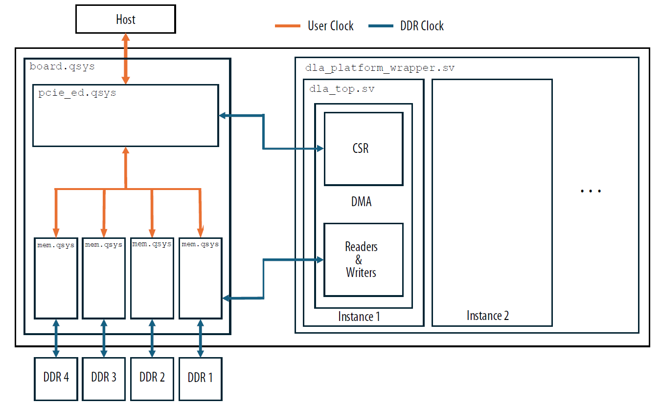
The board.qsys block contains two major elements; the pcie_ed.qsys block and the mem.qsys blocks. The pcie_ed.qsys block interfaces between the host PCIe data and the mem.qsys blocks. The mem.qsys blocks interface between DDR memory, the readers/writers, and the host read/write channels.
- Host read is used to read data from DDR memory and send it to the host.
- Host write is used to read data from the host into DDR memory.
- The MMIO interface performs several functions:
— DDR read and write transactions are initiated by the host via the MMIO interface
— Reading from the AFU ID block. The AFU ID block identifies the AFU with a unique identifier and is required for the OPAE driver.
— Reading/writing to the DLA DMA CSRs where each instance has its own CSR base address.
Note: Avalon MM/AXI4 adapters in Platform Designer might not close timing. Platform Designer optimizes for area instead of fMAX by default, so you might need to change the interconnect settings for the inferred Avalon MM/AXI4 adapter. For example, we made some changes as shown in the following figure.
Figure 3: Adjusting the Interconnect Settings for the Inferred Avalon MM/AXI4 Adapter to Optimize for fMAX Instead of Area.
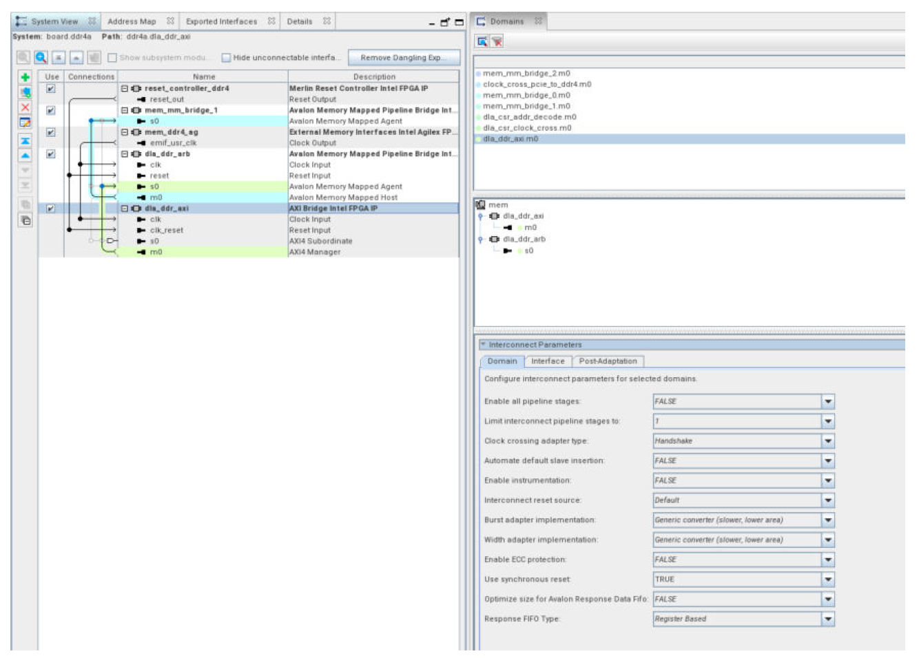
Note: This enables timing closure on the DDR clock.
To access the view in the above figure:
- Within the Platform Designer GUI choose View -> Domains. This brings up the Domains tab in the top-right window.
- From there, choose an interface (for example,
dla_ddr_axi). - For the selected interface, you can adjust the interconnect parameters, as shown on the bottom-right pane.
- In particular, we needed to change Burst adapter implementation from Generic converter (slower, lower area) to Per-burst-type converter (faster, higher area) to close timing on the DDR clock.
This was the only change needed to close timing, however it took several rounds of experimentation to determine this was the setting of importance. Depending on your system, other settings might need to be tweaked.
7.2.1 PLL Adjustment
The design example build script adjusts the PLL driving the FPGA AI Suite IP clock based on the fMAX that the Quartus Prime compiler achieves.
A fully rigorous production-quality flow would re-run timing analysis after the PLL adjustment to account for the small possibility that change in PLL frequency might cause a change in clock characteristics (for example, jitter) that cause a timing failure.
A production design that shares the FPGA AI Suite IP clock with other system components might target a fixed frequency and skip PLL adjustment.
Created: May 14, 2026