Nios V/g Lockstep System Example Design

Introduction
Nios® V/g Lockstep Design Example Design Overview
This design demonstrates the Nios V/g lockstep feature on Agilex® 7 FPGA F-Series Development Kit P-Tile and E-Tile DK-DEV-AGF014EA. It is based on UC_1 (Standard fail safe or No availability) control mechanism, with Nios® V/m as the system supervisor that injects root faults, reads alarms, and execute failure control mechanism.
The design is built with basic peripherals required for simple application execution:
- JTAG UART for serial output.
Prerequisites
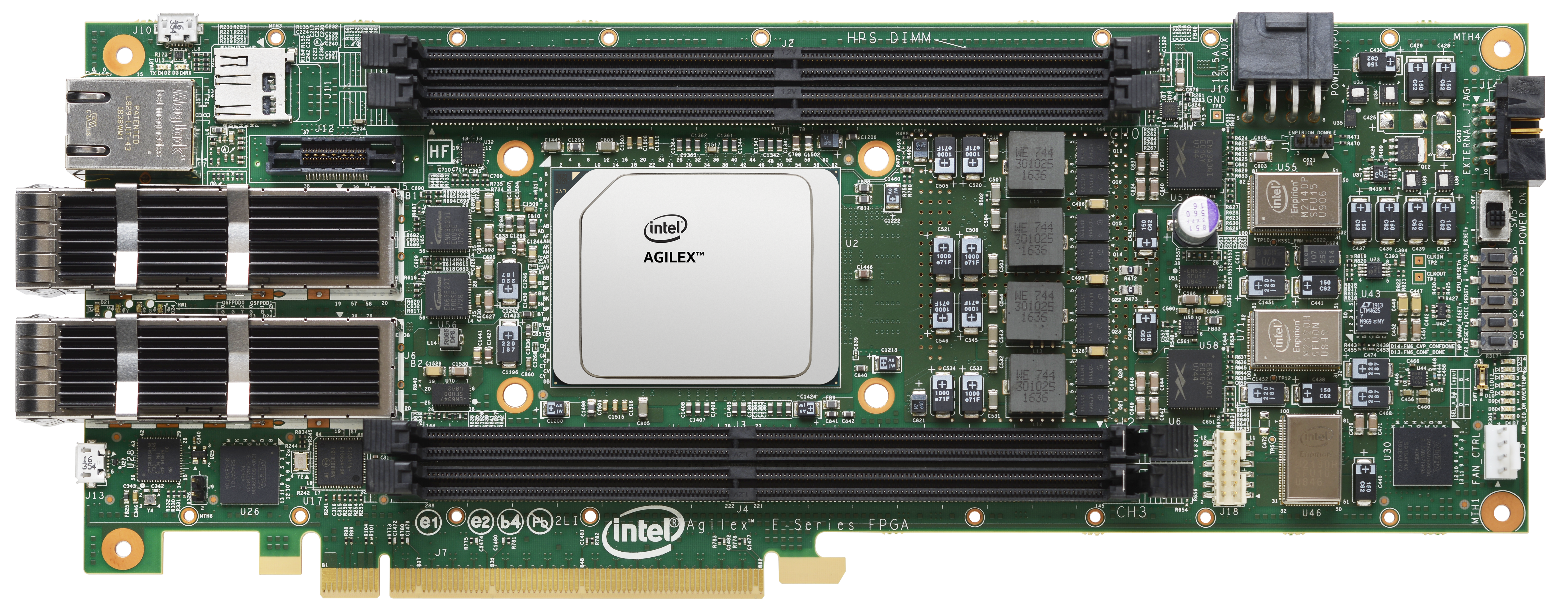
- Agilex® 7 FPGA F-Series Development Kit, ordering code DK-DEV-AGF014EA. Refer to the board documentation for more information about the development kit.
- Mini and Micro USB Cable. Included with the development kit.
- Host PC with 64 GB of RAM. Less will be fine for only exercising the prebuilt binaries, and not rebuilding the design.
- Quartus® Prime Pro Edition Software version 25.3.1
- Ashling* RiscFree* IDE for Altera® FPGAs
Release Contents
Every Nios V processor design example is maintained based on this folder structure. Here is the Github link to root directory of this design example: Nios® V/g Lockstep with Nios® V/m as System Supervisor Example Design Github link
---
title: Release Contents File Structure
config:
  flowchart:
    curve: linear
---

graph LR
    A[lockstep] --> B[docs]
    A --> C[img]
    A --> D[ready_to_test]
    A --> E[sources]
    B -->|contains| F{{Design Example MD file}}
    C -->|contains| G{{Figures or Illustrations}}
    D -->|contains| H{{Prebuilt Binary Files}}
    E --> I[hw]
    E --> J[scripts]
    E --> K[sw]
    I -->|contains| M{{Custom Hardware Design Files}}
    J -->|contains| N{{Scripts to Generate Hardware Design}}
    K -->|contains| P{{Custom Software Source Code}}
Nios® V/g Lockstep Design Design Architecture
This example design is made up of two subsystems:
- Target System: Nios® V/g Lockstep processor connected to its dedicated peripherals (On-Chip RAM II).
- System Supervisor: Nios® V/m processor connected to its dedicated peripherals (Reset Request PIO, On-Chip RAM II and JTAG UART IP).
- Shared peripherals between subsystems (Reset Acknowledgement PIO)
The objective of the design is to showcase the role of the System Supervisor in supervising the execution of the Target System.
The Target System runs a simple application that update the Reset Acknowledgement PIO to represents activity.
While the Target System is running, the System Supervisor:
- Polls the status of ALARMs of Target System.
- Triggers a false alarm within Target System through Root Fault Injection.
- Executes failure control mechanism on Target System using Reset Request (based on Reset Scenario 1 - CPUs and fRSmartComp asynchronous reset).
- Check the activity of Target System using the Reset Acknowledge PIO
The value in Reset Acknowledgement PIO indicates as follows:
- 00 >> System Supervisor is out-of-reset, but haven't send reset request to Target System.
- 01 >> System Supervisor resets Target System, and checks for Target System's activity.
- 02 >> Target System replies it is active.
- 03 >> The demonstration ends.
---
title: Design Block Diagram
config:
  flowchart:
    curve: linear
---

flowchart TB
subgraph top-level-subsystem
    Z[Clock Source]
    Y[Reset Source]

subgraph target-system
    A[Nios V/g Processor]
    A <--> C[On-Chip RAM II]
end
subgraph system-supervisor
    K[Nios V/m Processor]
    K <--> L[On-Chip RAM II]
    K <--> M[JTAG UART]
    K --> N[Reset Request]
    X[Reset Acknowledgement PIO]
end
end
Z --> system-supervisor
Z --> target-system
Y --> system-supervisor
N --> target-system
K --> |lockstep config| A
X --> K
A --> X
Nios® V/g Processor IP as the Lockstep Processor
- General-purpose 32-bit CPU for high performance applications with larger logic area utilization.
- Implements RV32IMZicsr_Zicbom instruction set (optionally with “F” and "Smclic" extension) instruction set.
- Supports five-stages pipelined datapath.
- It is a customizable soft-core processor, that can be tailored to meet specific application requirements, providing flexibility and scalability in embedded system designs.
Nios® V/m Processor IP as the System Supervisor
- 32-bit Microcontroller to achieve balance between performance and logic area utilization.
- Implements RV32I_Zicsr instruction set.
- Supports five-stages pipelined or non-pipelined datapath.
- It is a customizable soft-core processor, that can be tailored to meet specific application requirements, providing flexibility and scalability in embedded system designs.
Embedded Peripheral IP Cores
The following embedded peripheral IPs are used in this design:
- On-Chip RAM II IP
- JTAG UART IP
- PIO IP
System Components
The following components are used in this design:
- Clock Source (Clock Bridge with IO PLL)
- Reset Source (Reset Release IP)
Lockstep Processor Instance 0 Address Map Details (target-system)
| Address Offset | Size (Bytes) | Peripheral | Description |
|---|---|---|---|
| 0x0000_0000 | 256KB | On-Chip RAM Instance 1 | To store application |
| 0x0005_0050 | 16 | Reset Acknowledgement PIO | To report its activity |
System Supervisor Instance 1 Address Map Details (system-supervisor)
| Address Offset | Size (Bytes) | Peripheral | Description |
|---|---|---|---|
| 0x0000_0000 | 256KB | On-Chip RAM Instance 0 | To store application |
| 0x0005_0040 | 8 | JTAG UART Instance 1 | Communication between a host PC and the System Supervisor |
| 0x0005_0050 | 16 | Reset Acknowledgement PIO | To check Lockstep processor's activity |
| 0x0005_0060 | 16 | Reset Request PIO | Resets the Lockstep Processor |
| 0x0006_0000 | 64KB | Lockstep Processor | Access the Lockstep-related CSRs |
Development Kit Setup
Refer to Agilex® 7 FPGA F-Series Development Kit User Guide to setup the development kit.
Environment Setup
Download the Quartus® Prime Pro Edition and Ashling* RiscFree* IDE for Altera® FPGAs (software version 25.3.1) from the Quartus® Prime Design Software - Download from Altera website. Follow the on-screen instructions to complete the installation process.
Next, set up the Quartus® Prime Pro Edition and Ashling* RiscFree* IDE tools in the PATH.
export QUARTUS_ROOTDIR=~/altera_pro/25.3.1/quartus/
export PATH=$QUARTUS_ROOTDIR/bin:$QUARTUS_ROOTDIR/linux64:$QUARTUS_ROOTDIR/../qsys/bin:$QUARTUS_ROOTDIR/../riscfree/RiscFree:$QUARTUS_ROOTDIR/../niosv/bin/$PATH
Exercising Prebuilt Binaries
Program Hardware Binary SOF
- Connect the development kit to the host PC using USB Blaster II.
- Change the JTAG clock frequency to 6 MHz, and probe the JTAGServer to get the JTAG scan chain.
- Execute the quartus_pgm command to program the SOF file with the correct device number. Based on the JTAG scan chain below, the FPGA is at device number 1. You may require to provide a different device number if your JTAG chain is different from the given example.
jtagconfig --setparam 1 JtagClock 6M
jtagconfig -d
quartus_pgm --cable=1 -m jtag -o 'p;ready_to_test/top.sof@1'
For example:
1) AGF FPGA Development Kit
  C341A0DD   AGFB014R24A(.|R1|R2)/.. (IR=10)
  020D10DD   VTAP10 (IR=10)
    Design hash    5FDC6B667C01E6ADD7A4
    + Node 0C206E00  JTAG PHY #0

  Captured DR after reset = (4BA064770364F0DD020D10DD) [96]
  Captured IR after reset = (100555) [24]
  Captured Bypass after reset = (0) [3]
  Captured Bypass chain = (0) [3]
  JTAG clock speed auto-adjustment is enabled. To disable, set JtagClockAutoAdjust parameter to 0
  JTAG clock speed 6 MHz
Current Design State (Reset Acknowledgement PIO) = 0x0
Upon power‑on, System Supervisor is immediately released from reset, however, it is not executing any applications. Target System remains in reset and does not start operating until it receives reset‑release request from System Supervisor. Since the System Supervisor is idling, no reset-release request is sent.
Program Software Image ELF into System Supervisor
- Ensure that the development kit is successfully configured with the Hardware Binary SOF file.
- Launch the Nios V Command Shell. You may skip this if the shell is active.
- Execute the following command to download the ELF file into the System Supervisor (Instance 1).
Current Design State (Reset Acknowledgement PIO) = 0x1
System Supervisor begins its initialization sequence, and sends reset-release request to Target System (through Reset Request PIO). Target System is released from reset, however, it is not executing any applications. Since the Target System is idling, no reset-release acknowledgement is sent. This ensures that System Supervisor completes its necessary startup tasks before Target System becomes active.
Program Software Image ELF into Target System
- Ensure that the development kit is successfully configured with the Hardware Binary SOF file.
- Launch the Nios V Command Shell. You may skip this if the shell is active.
- Execute the following command to download the ELF file into the Target System (Instance 0).
Current Design State (Reset Acknowledgement PIO) = 0x2
Target System begins its initialization sequence, and sends reset-release acknowledgement to System Supervisor (through Reset Acknowledgement PIO). System Supervisor receives the reset-release acknowledgement. The Lockstep Mock Test begins.
Run Serial Console
You may proceed to to display the application printouts from System Supervisor (JTAG UART Instance 1), and verify the design.
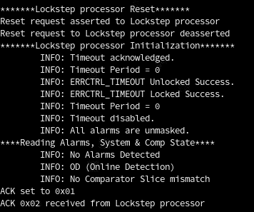
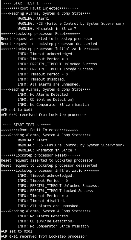
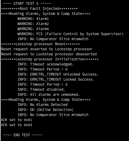
For example, you should see similar display at the start of the application.
Rebuilding the Design
Generate Project and Design Files
Run the following command in the terminal from the source directory. The script performs the following tasks, which generates the project and Platform Designer file of this design.
- Create a new project
- Create a new Platform Designer system
- Configure assignments and constraints
Generate Software Image ELF
After the hardware binary SOF file is ready, you may begin building the software design. It consists of the following steps:
- Create a board support package (BSP) project.
- Create a Nios® V processor application projects with the provided source code.
- Build the applications.
- Generate a software image ELF file.
Launch the Nios V Command Shell. You may skip this if the shell is active. Run the following command in the shell from the source directory.
Nios V/m processor as System Supervisor
niosv-shell
niosv-bsp -c --quartus-project=hw/top.qpf --qsys=hw/qsys_top.qsys --type=hal sw/bsp_lockstep/settings.bsp -i=intel_niosv_m_0
niosv-app --bsp-dir=sw/bsp_lockstep --app-dir=sw/app_lockstep --srcs=sw/app_lockstep/lockstep.c
cmake -S ./sw/app_lockstep -B sw/app_lockstep/build -G "Unix Makefiles"
make -C sw/app_lockstep/build
Nios V/g Lockstep processor as Target System
niosv-shell
niosv-bsp -c --quartus-project=hw/top.qpf --qsys=hw/qsys_top.qsys --type=hal sw/bsp_lockstep_hello/settings.bsp -i=intel_niosv_g_0
niosv-app --bsp-dir=sw/bsp_lockstep_hello --app-dir=sw/app_lockstep_hello --srcs=sw/app_lockstep_hello/hello.c
cmake -S ./sw/app_lockstep_hello -B sw/app_lockstep_hello/build -G "Unix Makefiles"
make -C sw/app_lockstep_hello/build
Program Hardware Binary SOF
- Connect the development kit to the host PC using USB Blaster II.
- Change the JTAG clock frequency to 6 MHz, and probe the JTAGServer to get the JTAG scan chain.
- Execute the quartus_pgm command to program the SOF file with the correct device number. Based on the JTAG scan chain below, the FPGA is at device number 1. You may require to provide a different device number if your JTAG chain is different from the given example.
jtagconfig --setparam 1 JtagClock 6M
jtagconfig -d
quartus_pgm --cable=1 -m jtag -o 'p;hw/output_files/top.sof@1'
For example:
1) AGF FPGA Development Kit
  C341A0DD   AGFB014R24A(.|R1|R2)/.. (IR=10)
  020D10DD   VTAP10 (IR=10)
    Design hash    5FDC6B667C01E6ADD7A4
    + Node 0C206E00  JTAG PHY #0

  Captured DR after reset = (4BA064770364F0DD020D10DD) [96]
  Captured IR after reset = (100555) [24]
  Captured Bypass after reset = (0) [3]
  Captured Bypass chain = (0) [3]
  JTAG clock speed auto-adjustment is enabled. To disable, set JtagClockAutoAdjust parameter to 0
  JTAG clock speed 6 MHz
Current Design State (Reset Acknowledgement PIO) = 0x0
Upon power‑on, System Supervisor is immediately released from reset, however, it is not executing any applications. Target System remains in reset and does not start operating until it receives reset‑release request from System Supervisor. Since the System Supervisor is idling, no reset-release request is sent.
Program Software Image ELF into System Supervisor
- Ensure that the development kit is successfully configured with the Hardware Binary SOF file.
- Launch the Nios V Command Shell. You may skip this if the shell is active.
- Execute the following command to download the ELF file into the System Supervisor (Instance 1).
Current Design State (Reset Acknowledgement PIO) = 0x1
System Supervisor begins its initialization sequence, and sends reset-release request to Target System (through Reset Request PIO). Target System is released from reset, however, it is not executing any applications. Since the Target System is idling, no reset-release acknowledgement is sent. This ensures that System Supervisor completes its necessary startup tasks before Target System becomes active.
Program Software Image ELF into Target System
- Ensure that the development kit is successfully configured with the Hardware Binary SOF file.
- Launch the Nios V Command Shell. You may skip this if the shell is active.
- Execute the following command to download the ELF file into the Target System (Instance 0).
Current Design State (Reset Acknowledgement PIO) = 0x2
Target System begins its initialization sequence, and sends reset-release acknowledgement to System Supervisor (through Reset Acknowledgement PIO). System Supervisor receives the reset-release acknowledgement. The Lockstep Mock Test begins.
Run Serial Console
You may proceed to to display the application printouts from System Supervisor (JTAG UART Instance 1), and verify the design.
For example, you should see similar display at the start of the application.
Created: April 29, 2026