Robotics Camera System Example Design — FPGA Hardware Functional Description
This document describes the functionality of the HPS_ISP_CAM_ROBOTICS hardware variant, using Platform Designer subsystems as a reference. The variant implements a robotics-oriented glass-to-glass camera path from the MIPI sensor through ISP to DisplayPort.
This page documents FPGA hardware subsystems, interconnect, and registers. Higher-level robotics software can run perception applications (for example ROS 2). A Nios® V core brings up the MIPI sensor, configures the ISP Lite and DisplayPort path, and services pipeline interrupts.
Platform overview
The Platform Designer system implements sensor ingest, real-time ISP, robotics frame export, and DisplayPort monitoring on the Agilex™ 5 device.
- The
clock_subsystemandboard_subsystemprovide reference clocks, resets, switches, and LEDs for the modular development kit. - The
hps_subsystemis the Agilex™ 5 Hard Processor System with DDR4 EMIF, UART, Ethernet, I2C, SD, and HPS-to-FPGA bridges. Linux configures ISP Robotics CSRs on the lightweight bridge and reads frame buffers on the full bridge (or via MSGDMA). - Vision subsystems:
MIPI In,ISP In,ISP Lite,ISP Robotics,ISP Lite Out, anddp_tximplement the live path from the Framos FSM:GO IMX678C Camera Modules to DisplayPort 1.4 at up to 4Kp30. ISP Robotics scales the stream and writes 960×540 grayscale and RGB branches to FPGA DDR for software. A Nios® V subsystem programs MIPI, ISP In, ISP Lite, ISP Lite Out, and DisplayPort CSRs. - EMIF subsystem 1 and EMIF subsystem 2: DDR4 frame stores on banks 2B and 3B for robotics and display buffering.
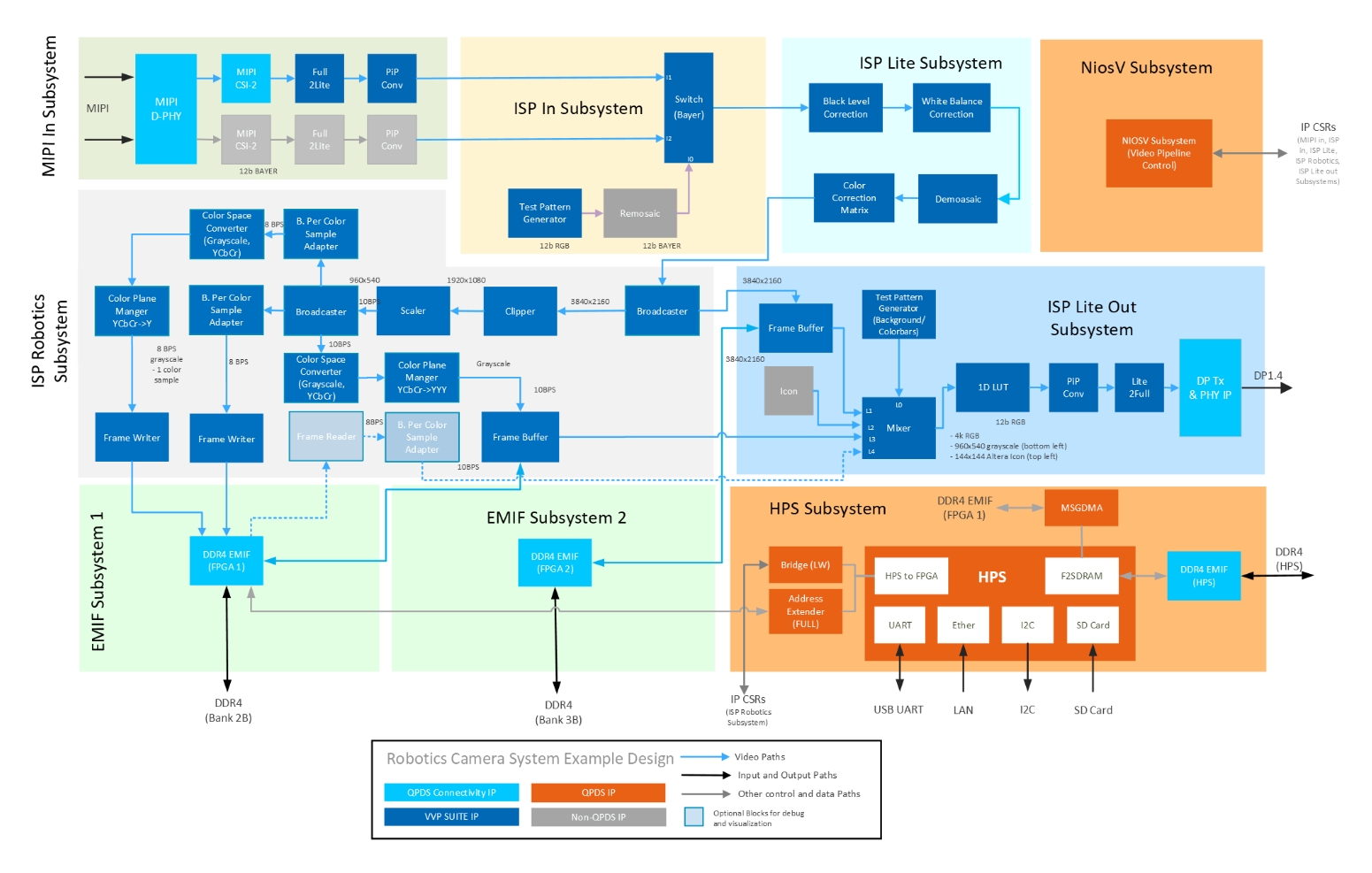
High-Level Hardware Block Diagram of the Robotics Camera System Example Design.
Blue interconnect in the diagram is the live video path (MIPI In → ISP In → ISP Lite → ISP Robotics → ISP Lite Out → DisplayPort). Grey paths are control and memory access from the Nios® V and HPS subsystems.
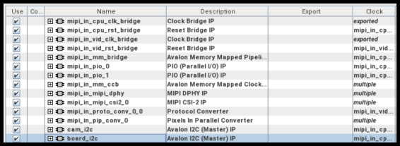
The diagram is color-coded to match the Platform Designer view and the XML file (Modular Design Toolkit methodology) for this design (see: AGX_5E_Modular_Devkit_HPS_ISP_CAM_ROB.xml). The following figure correlates the XML file, and the Platform Designer view:
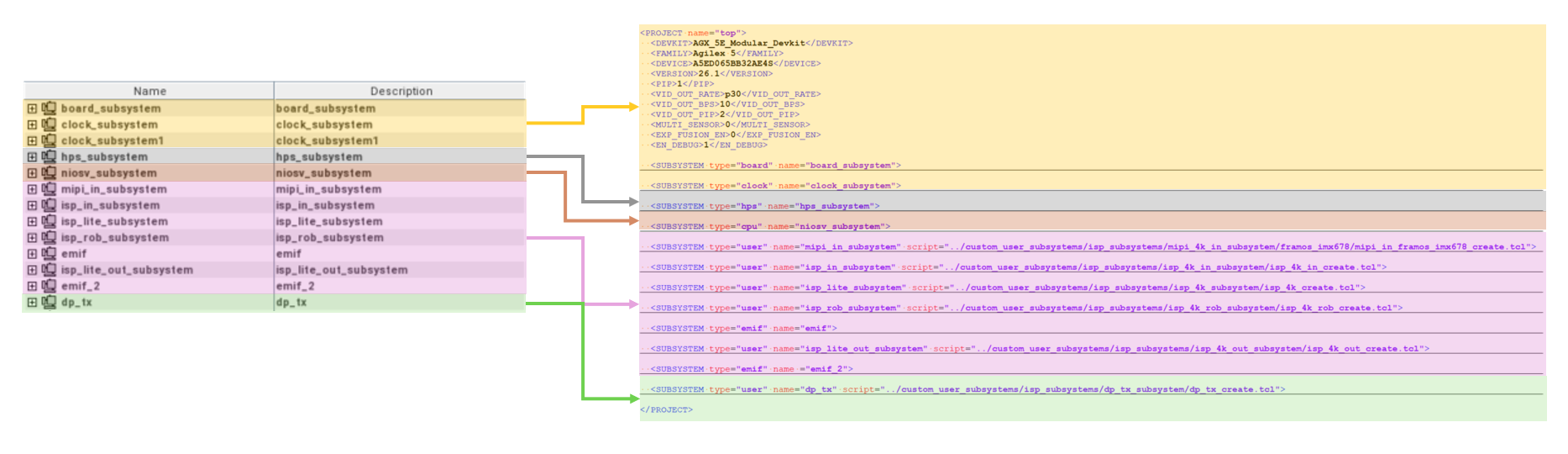
Modular Design Tool Kit PD project vs XML file.
Hardware subsystems and components
Clock and board subsystems
The clock subsystem and board subsystem contain IP related to modular development kit resources: buttons, switches, LEDs, reference clocks, and resets. They forward clocks and resets to the MIPI, ISP, DisplayPort, and HPS subsystems. These are shared MDT building blocks, consistent with other camera and robotics example designs.
Board and Clock Subsystems PD sub-Blocks.
This variant uses a single clock_subsystem with multiple generated clocks (for example 297 MHz, 148.5 MHz, and
200 MHz domains) to satisfy MIPI, ISP, DisplayPort, and EMIF timing.
HPS subsystem
The HPS subsystem is an instance of the Hard Processor System Agilex™ 5 FPGA IP, configured consistently with the Agilex™ 5 E-Series Modular Development Kit GSRD User Guide (26.1). The design boots a Yocto-based Linux image built.
Internally the subsystem includes:
- HPS DDR4 EMIF for the on-board SOM memory used by software paths.
- Lightweight and full HPS-to-FPGA AXI bridges. ISP Robotics CSRs (frame writers, clipper, scaler, and
related blocks) map to the lightweight bridge (MPU base
0x2000_0000). Frame pixel data in FPGA DDR is accessed through the full bridge and optionally mSGDMA. - Modular Scatter-Gather DMA (mSGDMA) for memory-to-memory frame movement on the robotics ISP path.
Hard Processor System (HPS) PD sub-Block.
The lightweight HPS-to-FPGA bridge (base 0x2000_0000) exposes ISP Robotics control registers to Linux and UIO
drivers. The full HPS-to-FPGA bridge provides high-bandwidth access to frame buffers in EMIF subsystem 1
(MPU window starting at 0x6000_0000; see below).
Vision pipeline subsystems
The vision path follows the streamlined ISP Lite style. Video and vision IP blocks come from the VVP IP Suite; see the Video and Vision Processing Suite Altera® FPGA IP User Guide for block-level IP documentation.
MIPI In subsystem
The MIPI In subsystem is the primary video source for this example. It connects a Framos FSM:GO IMX678C Camera Modules
on the kit MIPI connector through MIPI D-PHY and MIPI CSI-2 receive IP, with format conversion to produce a 12-bit
Bayer stream in FPGA fabric. Sensor power and I2C setup are exposed through PIO and I2C controller agents, initialized by
the Nios® V pipeline controller during bring-up (configuration profile cfg_sensor in software_rob).
MIPI In Subsystem PD sub-Blocks.
ISP In subsystem
The ISP In subsystem provides a Switch (Bayer) to select live MIPI sensor data or a Test Pattern Generator path (color bars, via Remosaic) for pipeline debug without a camera attached. For normal operation, select the MIPI path after the sensor is powered and configured.
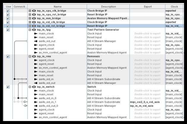
ISP In Subsystem PD sub-Blocks.
ISP Lite subsystem
The ISP Lite subsystem performs first-stage Bayer conditioning:
- Black level correction
- White balance
- Demosaic
- Color correction matrix (Bayer to RGB)
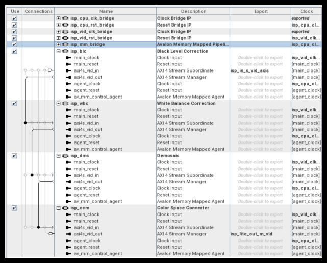
ISP Lite Subsystem PD sub-Blocks.
This stage matches the Camera Lite philosophy: a focused real-time path without tone-mapping, HDR merge, or multi-exposure blocks of the full 4K HDR camera solution.
ISP Robotics subsystem
The ISP Robotics subsystem adds robotics-oriented processing on the RGB stream from ISP Lite.
- Clipper and Scaler: produce reduced-resolution branches (for example from 3840×2160 toward 1920×1080 and 960×540) for lower-bandwidth software consumption.
- Color space converter and color plane merger: derive 8-bit and 10-bit grayscale streams for vision workloads.
- Frame writer, frame reader, and frame buffer: connect to
EMIF subsystem 1so the HPS can read processed frames through the full bridge and MSGDMA. - Frame writer (low res, grayscale) and frame writer (low res, RGB): export 960×540 frames for
Linux (for example
sensor_msgs/Imagemono8on/robotics_camera/image_raw).
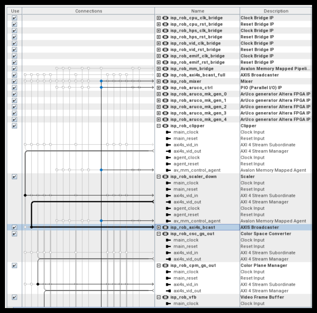
ISP Robotics Subsystem PD sub-Blocks.
HPS control (lightweight bridge)
ISP Robotics blocks that Linux configures are on the lightweight HPS-to-FPGA bridge (MPU base 0x2000_0000):
| Block | Offset from lightweight base (0x2000_0000) |
MPU address |
|---|---|---|
| Frame writer (low res, RGB) | 0x0000_0200 |
0x2000_0200 |
| Frame writer (low res, grayscale) | 0x0000_0800 |
0x2000_0800 |
Frame pixel data is not on the lightweight bridge; it resides in EMIF subsystem 1 and is reached through
the full bridge (see EMIF subsystems below).
Frame writer (low res, RGB and grayscale)
Both low-resolution frame writers share the same VVP frame-writer CSR map (see the Video and Vision Processing Suite Altera® FPGA IP User Guide).
Offsets in the table below are relative to each block’s base (0x2000_0200 for RGB, 0x2000_0800 for grayscale).
| Offset | Register | Access | Description |
|---|---|---|---|
0x0100 |
IRQ_CONTROL | R/W | Interrupt control |
0x0104 |
IRQ_STATUS | R | Interrupt status |
0x0120 |
IMG_INFO_WIDTH | R/W | Image width (default 960) |
0x0124 |
IMG_INFO_HEIGHT | R/W | Image height (default 540) |
0x0140 |
STATUS | R | Frame writer status |
0x0164 |
COMMIT | R/W | Commit pending CSR writes |
0x0168 |
BUFFER_ACKNOWLEDGE | W | Write 0x1 to commit a frame write to memory |
0x016C |
RUN | R/W | Run mode (see below) |
RUN (0x016C) values:
| Value | Mode |
|---|---|
0 |
Frame writer stopped |
1 |
Frame writer free-running |
2 |
Frame writer stopped |
3 |
Frame writer single-shot |
ISP Lite Out subsystem
The ISP Lite Out subsystem buffers the main 4K display path. A Mixer composites the full-resolution RGB stream with the scaled 960×540 grayscale preview, an optional Altera icon overlay, and test patterns. DP Tx and PHY drive DisplayPort 1.4 at up to 4Kp30 for local monitoring.
DisplayPort (dp_tx subsystem)
The dp_tx subsystem contains DisplayPort transmitter IP and board I2C for the DP link. The Nios® V/m application
configures the mode table and link training; see software_rob under the Quartus project.
Nios® V subsystem (video pipeline control)
A Nios® V soft-processor subsystem acts as the video pipeline controller. It programs IP CSRs in MIPI In,
ISP In, ISP Lite, ISP Lite Out, and DisplayPort during boot and runtime. The HPS owns CSR programming and
frame access for the ISP Robotics path. Refer to the software directory in the Quartus project (cfg_sensor build profile).
EMIF subsystems (vision frame stores)
EMIF subsystem 1 (DDR4 bank 2B) holds the robotics frame buffers written by ISP Robotics. EMIF subsystem 2
(DDR4 bank 3B) backs the higher-resolution display pipeline in ISP Lite Out and DisplayPort. Both are separate
from the HPS DDR4 EMIF used by the HPS.
In the default 960×540 configuration, EMIF subsystem 1 exposes two buffers for HPS software:
| Buffer | Format | Size (pixels) | Bytes per frame | Offset in FPGA EMIF window | HPS access (full bridge) |
|---|---|---|---|---|---|
| Grayscale (luma) | Single-plane 8-bit (mono8-style) | 960 × 540 | 518,400 (0x7E900) |
0x0020_0000 |
0x6020_0000 |
| RGB | 8 bits per color sample (R, G, B) | 960 × 540 | 1,555,200 (0x17B000) |
0x0000_0000 |
0x6000_0000 |
Frame size calculations:
- Grayscale: 960 × 540 × 1 byte/sample = 518,400 bytes.
- RGB: 960 × 540 × 3 bytes/pixel = 1,555,200 bytes (line stride 2880 bytes in the frame writer configuration).
The HPS reaches FPGA DDR through the full HPS-to-FPGA bridge. The FPGA EMIF window is at offset 0x2000_0000
from the bridge base (0x4000_0000), so EMIF subsystem 1 appears at MPU address 0x6000_0000. Linux maps
the buffer regions through UIO; ISP Robotics CSRs remain on the lightweight bridge at 0x2000_0200 and 0x2000_0800.
EMIF subsystem 2 supports the 4K display path in ISP Lite Out, not the exported robotics buffers above.
Created: June 25, 2026